تولید نخستین لیزر پرتوایکس اتمی

بعد از انتظاری ۴۵ساله، دانشمندان مرکز شتاب‌دهنده خطی استنفورد (SLAC) وابسته به وزارت انرژی آمریکا، موفق به تولید خالص‌ترین و کم‌بسامدترین لیزر پرتو ایکس شدند؛ دستاوردی که نوید موجی جدید از کشفیات علمی را می‌دهد.

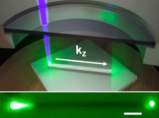
به گزارش نیچر، این پژوهشگران با تمرکز دادن پرتوهای تولیدشده در "چشمه نور همدوس شتاب‌دهنده خطی" (LCLS) وابسته به مؤسسه SLAC، بر یک کپسول حاوی گاز نئون، موفق به تحریک یک جریان آبشارمانند از پرتوهای ایکس و لذا تولید نخستین "لیزر پرتو ایکس اتمی" جهان شدند. به‌گفته نینا رورینگر (Nina Rohringer)، فیزیکدانی از کارگروه مطالعات پیشرفته انجمن ماکس پلانک آلمان‌ که سرپرستی این پژوهش را عهده‌دار بوده است، "پرتوهای ایکس، دید نافذی را به درون دنیای اتم‌ها و مولکول‌ها می‌کشانند." رورینگر و گروهش، این پژوهش را با همکاری محققانی از دانشگاه ایالتی کلرادو و نیز آزمایشگاه ملی لارنس لیورمور آمریکا به ثمر رساندند.
 
وی می‌افزاید: "روزی را می‌بینیم که محققان، این نوع جدید از لیزر را در حوزه‌های گوناگون و جذابی نظیر بررسی جزئیات واکنش‌های اتمی، یا تماشای مستقیم فعل و انفعالات زیستی در ابعاد مولکولی به کار گیرند. هرچه بسامد لیزر کوتاه‌تر باشد، می‌توان فعل و انفعالات را سریع‌تر و هر چه خلوصش بیشتر باشد، جزئیات ریزتری را زیر نظر گرفت."
 
از سال ۱۹۶۷ میلادی پیش‌بینی شده بود که می‌توان از روشی شبیه به فرآیند تولید لیزر نوری- یعنی تحریک کردن الکترون‌ها به فروریزش از ترازهای اتمی ِ پرانرژی به ترازهای کم‌انرژی‌تر که به آزادسازی یک فوتون می‌انجامد- دست به ساخت لیزر پرتوایکس هم زد، اما تا سال ۲۰۰۹ که LCLS به راه افتاد، هیچ منبع پرتوایکسی نبود که قدرت لازم برای تولید چنین نوعی از لیزر را داشته باشد.
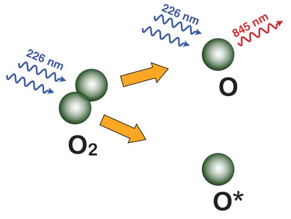
در فرآیند تولید لیزر اتمی، پالس‌های پرقدرت پرتوایکس که توسط LCLS تولید می‌شد- و هرکدام‌شان یک میلیارد بار درخشنده‌تر از نمونه‌های قبلی بودند- موجب آزادسازی الکترون‌های موجود در ترازهای میانی بخش اعظمی از اتم‌های نئون می‌شدند. ترازهای خالی اتم‌های نئون، در دو درصد از موارد توسط الکترون‌های آزاد پر می‌شد. این الکترون‌ها نیز انرژی‌شان را با گسیل یک فوتون پرقدرت پرتوایکس آزاد می‌کردند. فوتون‌های تولیدشده، اتم‌های همجوار را تحریک می‌کردند و با به راه انداختن یک جریان دومینومانند، انرژی پرتو تولیدشده را که همان لیزر پرتو ایکس اتمی باشد تا ۲۰۰ میلیون برابر انرژی القایی افزایش می‌دادند.
 
هرچند که پرتو القایی و پرتو تولیدی، هردوی‌شان از نوع لیزر هستند، اما فرآیندهای تولید نورشان با هم متفاوت است و نورشان هم خواص یکسانی ندارد. LCLS، با عبور دادن الکترون‌های پرانرژی از درون میدان‌های مغناطیسی متناوب موفق به تولید لیزر پرتو ایکس می‌شود که بسامد و همچنین درخشندگی‌اش از پرتوهای ایکس معمولی بیشتر است، اما لیزر پرتو ایکس اتمی، نه‌تنها بسامدش معادل یک‌هشتم لیزر پرتو ایکس غیر اتمی است، خلوص بیشتری دارد و واجد کیفیاتی است که آن را قادر به تمیز جزئیات واکنش‌های فوق سریع می‌کند؛ امکانی که تا پیشتر میسر نبود.
 
جان بوزک (John Bozek)، از دانشمندان LCLS می‌گوید: "این موفقیت، راه را به روی قلمروی جدید از توانمندی‌های پرتو ایکس گشود. مطمئناً دانشمندان خواهان مجهز شدن به ابزارآلاتی‌اند که این نوع از لیزر را به کار بگیرد." مثلاً محققان امید دارند که روزی بشود از لیزر LCLS و نیز لیزر اتمی، در یک پژوهش دوسویه استفاده کرد: یعنی کاری کرد که لیزر اولی، باعث بروز دگرگونی‌هایی در نمونه تحت بررسی شود و بعد از آن، لیزر دومی، دگرگونی‌های رخ‌داده را با دقتی معادل یک‌کوادریلیونیم ثانیه، به ثبت برساند. به‌گفته رورینگر، پژوهش‌های بعدی معطوف به تولید لیزرهای پرتو ایکس کم‌بسامدتر از طریق القای انرژی به اتم‌های اکسیژن، نیتروژن و گوگرد خواهد بود.
 
ترجمه از احسان سنایی

الماس زیر نور خورشید ناپدید می شود

الماس یکی از سخت ترین مواد شناخته شده است ولی نکته بسیار جالب در اینجا است اگر یک الماس را در مسیر نور خورشید قرار دهیم , شروع به از دست دادن اتم های خود می کند. نرخ کاهش اتم ها به قدری نیست که جواهرسازان یا دارندگان حلقه های برلیان را نگران کند، ولی کشف این موضوع قطعا راه استفاده از خواص استثنایی اپتیکی و الکترونی الماس را برای محققان آسانتر می سازد. بسیاری از کاربردهای جدید الماس از کاربرد آن در تابش های لیزری گرفته تا کاربرد آن در ارتباطات و محاسبات کوانتومی نیازمند ساختارهای ریزی در ابعاد میکرو و نانو برروی سطح الماس است.

ریچ میلدرن (Mildren Rich ) و گروهش در دانشگاه مک گوایر سیدنی نشان داده اند که استفاده از پرتو های فرابنفش راه بسیار خوبی برای این کار است. الماس ها معمولا به کمک لیزر قلم زنی می شوند (etching) و در این فر آیند اتم های روی سطح آن سوزانده شده و یک سطح ناهموار که بیشتر به گرافیت شباهت دارد تا به الماس را به وجود می آورند . میلدرن و همکارانش هنگامی که در حال ارتقا دادن ویژگی های لیزرهای ساخته شده از الماس بودند به صورت کاملا تصادفی متوجه شدند که با قطع کردن پرتوی تابشی فرآیندی که به جداشدگی (desorpton) معروف است آغاز شده و اتم های برانگیخته شده روی سطح الماس ناپدید شده و نهایتا سطح صاف و تراش خورده ای باقی می ماند . میلدرن می گوید:"ما می خواستیم نشان دهیم که الماس (الماس استفاده شده در لیزر) می تواند در طول موجهایی کار کنند که مواد دیگر نمی توانند و البته فرابنفش هم یکی از این نواحی است" .

این گروه موفق شدند لیزری از جنس الماس بسازند که اشعه فرابنفش ساطع کند اما تنها نقص این لیزر در مدت کارکرد آن است. این لیزر پس از 10 دقیقه از کار می ایستد. میلدرن اضافه می کند که : "به نظر می رسد که ما به وجود آوردن سوراخ های کوچکی روی سطح الماس می توانیم اتم های کربن را آزاد کنیم."

معمای غیر قابل حل الماس

اینکه چه گونه فرآیند جداشدگی اتفاق می افتد باید بررسی شود اما میلدرن دو نظریه دارد که در نشریه مواد اپتیکی (Express Material Optical) به چاپ رسیده است .

اولین نظریه این است که فرآیند جداشدگی نیازمند این است که سطح الماس با اتم های اکسیژن پوشانده شده باشد . دومین فرض او این است که برای آزاد شدن یک اتم کربن به دو فوتون نیاز داریم . هنگامی که 2 فوتون به سطح الماس برخورد کند , یک برانگیختگی در سطح الماس به وجود می آید و جفت الکترون و حفره برانگیخته شده‌ی داخل الماس می توانند تابش کنند و در نهایت این فرآیند می تواند اتم کربن را آزاد کند. میلدرن می گوید:"انرژی برانگیختگی بیشتر از مقدار انرژی لازم برای ناپدید شدن یک مولوکول کربن مونواکسید است . همچنین امکان دارد که اشعه فرابنفش مستقیما از سطح الماس منتشر گردد که منجر به شکستگی قیود شده و کربن مونواکسید آزاد شود ."

پروژه میلدرن اولین کار تحقیقاتی بر روی جزییات روند قلم زنی است و نشان می دهد که رابطه بین نرخ جذب دو فوتون و سرعت قلم زنی (به عبارتی خراش دادن سطح) تا حد بسیار خوبی خطی است که به ما کمک می کند کنترل نرخ خراشیدگی را در دست بگیریم. آزاد شدن کربن حتی می تواند در زیر نور خورشید هم رخ دهد . اگرچه سرعت از دست دادن اتم ها بسیار آرام است به گونه ای که حتی برای یک لامپ فرابنفش جیوه در آزمایشگاه ده بیلیون سال طول می کشد که یک میکروگرم از الماس را از بین ببرد .

بنا به گفته استیون پراور (Prawer Steven ) سرعت بسیار کم از دست دادن اتم ها امکان استفاده از این روش را به عنوان تکنیکی برای صیقل دادن سطح الماس محدود می سازد. استیون پراور تحقیقات روی مواد در دانشگاه ملبورن استرالیا را سرپرستی می کند . او می گوید : "گفتن این جمله که استفاده از این روش مناسب نیست درست به نظر نمی رسد .ما قادر خواهیم بود با ترکیب این روش با روش فرسایش، سطح خراشیده شده را صیقل دهیم."

پراور برای اولین بار سعی دارد در زمینه ارتباطات کوانتومی و مخابره کردن اطلاعات ازلیزر ساخته شده از الماس که تک فوتون ساطع می کند استفاده کند و برای این منظور داشتن سطح صاف برای الماس استفاده شده ضروری است. پراور می گوید : "برای گیر انداختن نور می بایست داخل موجبر فوتون تولید کنیم اما نشانه گذاری بر روی موجبر باعث به وجود آمدن سطح ناهموار می شود و سطوح ناهموار باعث پراکنده شدن نور می شوند و این بدان معنی است که با این روش نتایج لازم را به دست نمی آوریم."

لینک منبع

Polariton coupling becomes stronger

Researchers at the University of Pennsylvania in the US claim that polaritons – quasiparticles that are part matter and part light – couple more strongly when confined in nanoscale semiconductors. The new result could benefit photonic circuits that exploit light rather than electricity.

A polariton is a particle-like entity (or quasiparticle) that can be used to describe how light interacts with semiconductors and other materials. It has two different components: an electron-hole pair (or "exciton") and a photon, which is emitted when the electron and hole recombine. When a photon is emitted, it is immediately reabsorbed to reform an exciton, so the cycle is repeated. This continuous exchange, or coupling, of energy between photons and excitons can be described in terms of polariton states.

Polaritons are expected to play an important role in future photonics devices that would use light instead of electricity to process information. Such devices would be much faster and use less energy than their electronic counterparts. The strong coupling of polaritons will be crucial for the success of this new photonics, but the coupling strength of polaritons in bulk semiconductors was always thought to be limited by the properties of the semiconductor material itself.

The right finishing techniques

Ritesh Agarwal and colleagues are now saying that this limit can be overcome if the right fabrication and finishing techniques are used to make the semiconductor structures in question. This is because the light-matter coupling strength increases dramatically as semiconductors become smaller than 500 nm or so, explains Agarwal.

"When you're working at bigger sizes, the surface is not as important," he said. "The surface to volume ratio – the number of atoms on the surface divided by the number of atoms in the whole material – is a very small number. But when you make a very small structure, say 100 nm, this number is dramatically increased. Then what is happening on the surface critically determines the device's properties."

Although researchers had previously attempted to make polariton cavities on such a small scale, the "top-down" chemical etching methods employed to fabricate the devices damaged the semiconductor surfaces, so creating defects. These defects trapped the excitons, making them unavailable for transporting current.

Self-assembling nanowires

Agarwal's team overcame this problem by self-assembling nanowires made from cadmium sulphide instead of etching nanoscale structures. Surface quality was still an issue, even with this fabrication technique, so they developed a way to "passivate" the surface of the nanowires by growing a silicon oxide around them. This greatly improved the optical properties of the wires because the oxide shell fills the electrical gaps in the nanowire surface and prevents the excitons from getting trapped on the surface, says Agarwal.

The scientists also developed techniques (based on detecting the energy of standing waves formed in the nanowire cavities) for measuring the light-matter coupling strength and showed that it was indeed enhanced as the semiconductor structures became smaller. Stronger light-matter coupling means faster photonic switches and much more efficient polariton lasers, light-emitting diodes and amplifiers – to name a few possible applications.

However, not all scientists are convinced of the team's results. Benoit Deveaud-Plédran of École Polytechnique Fédérale de Lausanne described the team's claims as "overstated" and said that they don't appear to be backed up by data presented in a paper outlining the experiment (PNAS 108 10050 ).

Others are more enthusiastic. "This paper looks like an interesting addition to the armoury of light-matter strong coupling effects in semiconductors," commented Jeremy Baumberg of the University of Cambridge's Cavendish Laboratory in the UK. "The results show a new way to reduce the volume of the microcavity, by using high refractive index nanowires, which tightly confine the light inside. The rate at which energy is flipped back and forth between light and excitons depends on inverse square root of the volume within which the light is trapped. Here the wall of the semiconductor is used to confine the light, and it is tighter than normal, giving rise to faster rates and thus a higher splitting between the polariton 'modes'."

Improvements needed

It is an interesting new route to making strong coupled systems at room temperature, he told physicsworld.com, but the design might not be more than just "fortuitous", Baumberg cautions. The light leaks out from the structure in many directions, and is not confined well enough to keep the resonances narrow. "Improvements will rely on much better control of the length, width, orientation and out-coupling of light from nanowires," he added.

Other teams around the world are also looking at new ways of achieving room temperature strong polariton coupling. Baumberg's group, for its part, has recently published a paper in Applied Physics Letters describing a set-up that comprises air suspended mirrors and simpler semiconductors based on the well known gallium arsenide. This system has light out-coupled in only vertical directions and it can be electrically controlled.

Physicists create 'anti-laser'

In a fascinating case of physics being turned on its head, a group of researchers at Yale University in the US has created an "anti-laser" that almost perfectly absorbs incoming beams of coherent light. The invention is based on a theoretical study reported last summer in which Douglas Stone and his Yale colleagues claimed that such a system could be possible in a device that they call a coherent perfect absorber (CPA). Instead of generating coherent light beams with a laser, the devices absorb incoming coherent light and convert it into either heat or electricity.

Now, having teamed up with experimental physicists at Yale, Stone has built a version of the device by creating an "interference trap" inside a silicon wafer. Two laser beams – originally split from a single beam – are directed onto opposite sides of the wafer and their wavelengths are fixed so that an interference pattern is established. In this way, the light waves get stalled indefinitely, bouncing back and forth within the wafer, with 99.4% of both beams being transformed into heat.

The group argues that there is no theoretical reason why 100% of the light could not be absorbed using the technique. The researchers are also confident that the current size of the device, 1 cm in diameter, can be reduced to just 6 µm. "It is surprising that the possibility of the 'time-reversed' process of laser emission has not been seriously discussed or studied previously," says Stone.

Focus on applications

Stone's group believes that its "anti-laser" could prove to have many exciting applications. These might include filters for laser-based sensors at terahertz frequencies for sniffing out biological agents or pollutants, which requires detecting a small backscattered laser signal against a large background of thermal noise.

Another idea is to use the device as a type of shield in medical applications to enable surgeons to fire laser beams at unwanted biological tissue, such as tumours, with greater accuracy. "With our technique an appropriately engineered incident set of light waves could penetrate deeply into such a medium and be absorbed only at the centre, enabling delivery of energy to a specified region," explains Stone.

The group also speculates that by adding another "control" beam it could control the device to toggle between near complete absorption and 1% absorption. This property could enable the devices to function as optical switches, modulators and detectors in semiconductor integrated optical circuits.

One limitation of all such devices, however, is that they will only work at specific wavelengths, meaning that the technology will not be particularly useful in photovoltaic cells or cloaking devices.

Physicists create 'backward laser'

A team of physicists in the US has created an infrared laser beam at a point in mid air, by focusing a UV laser onto a tiny volume of oxygen molecules. Much of the emergent infrared laser light travels back towards the UV laser, sampling the intervening air as it returns. As such, this "backward laser" could potentially provide measurements of pollutants and other molecules in environments that would be hard or impossible to study with conventional laser systems.

There are a number of different ways in which lasers are used to measure the concentration of particular gases in the air, be it pollutants in the atmosphere or the trace gases given off by solid explosives. These techniques include Raman scattering, in which light returns with a shift in wavelength as a result of atomic or molecular laser excitation. However, the scattered light is extremely weak and therefore yields a very low signal. In "stimulated Raman gain", the signal is enhanced by exciting the gas molecules so that they emit at the same frequency as the laser. This requires the detector to be positioned on the far side of the gas sample, which makes its use in some enclosed or remote environments very difficult.

One way to get round this limitation is to set up a laser in mid-air, its beam sampling the molecules along its path as it returns to the source. In 2004 a group led by See Leang Chin of Laval University in Canada used an infrared laser to ionize nitrogen atoms, the recombining ions and electrons then emitting light coherently. However, this approach calls for a very powerful laser, and Chin's group obtained only a very small gain coefficient, which means the researchers had to ionize a long stretch of air to get any significant lasing action.

Population inversion

In the latest work, Richard Miles and colleagues at Princeton University used a different mechanism to set up mid-air lasing. By focusing a 226 nm wavelength laser beam onto a tiny volume of air at a distance of between 30 cm and 1 m, they were able to break down oxygen molecules into their constituent atoms and then excite these atoms. Getting these atoms to lase then relied on two crucial properties of the beam’s focus. Being very high intensity, this focus induces a population inversion in the oxygen atoms, ensuring that there are more excited than non-excited atoms.

In addition to this, the shape of the focus – being about a millimetre long and just a hundredth of a millimetre wide – means that any atoms undergoing spontaneous emission tend to stimulate emission in other excited atoms either in the forward or backward directions, rather than at some arbitrary angle to the beam. This leads to high gain in both forward and backward directions.

To confirm that they had indeed generated backward lasing, the researchers placed a CCD detector a metre behind the focus and then placed a more sensitive photomultiplier tube at arbitrary angles to the beam. They found that the brightness behind the focus was some million times higher than that in other directions.

Inspired by hot flames

According to Miles's colleague, Arthur Dogariu, the inspiration for their backward laser came a few years ago when they were using the same 226 nm laser to study the creation of atomic oxygen inside hot flames. They were using the laser to excite and ionize the atoms liberated by the heat of the flame in order to measure the characteristic emissions of different flames. But what they noticed was that even when they turned the flame off they were still getting a signal – in other words, the laser was breaking up as well as exciting the oxygen.

The researchers now plan to optimize their set-up to see how much higher than can raise the gain of their backward laser. Then they will try and detect various molecules using a number of different detection schemes, including stimulated Raman gain. They say that their backward laser would, for example, make it much easier to scan the atmosphere for signs of methane in the case of a ruptured gas pipe. Alternatively, they say it could be used to enhance the detection of explosives by probing the air around suspect packaging, increasing the distance and reducing the concentrations at which such an analysis could be carried out compared with standard Raman scattering.

Real-world measurements

Chin describes the work as "very interesting" but says he is not yet convinced that such backward lasing could actually be used to detect pollutants and other gases. He maintains that the researchers have not adequately explained how the principle would work with molecules other than oxygen and also cautions that the small-scale laboratory results cannot necessarily be extrapolated to the much larger distances involved in real-world measurements.

Miles Padgett of Glasgow University shares Chin's sentiment. He says the research is "quite fascinating," but adds that "for my money the excitement is the effect itself rather than a possible application at this stage".

يك پلاسماي معلق در اثر دشارژ الکتریسیته

Image Credit: Caroline J. v. Wurden and Glen A. Wurden, Los Alamos

پلاسما

تقریبا ً همه در پاسخ به این پرسش که ماده چند حالت دارد، می گویند سه حالت: جامد، مایع و گاز. ولی چنین نیست گازها در درجه حرارت های بسیار بالا، حالت چهارم ماده را پدید می آورندکه پلاسما نامیده می شود. پلاسما چنانکه که شایسته آن است شناخته نشده، با این حال همه جا می توان آنرا یافت. در جهان از ماده ستارگان گرفته تا پرتوهای کیهانی و در اطراف کره خاکی، درون حوزه مغناطیسی زمین، ماده در حالت پلاسما وجود دارد.

پلاسما چیست؟ پلاسما گازی است که از ذرات باردار تشکیل شده است. در واقع گازها در درجه حرارت های بالا، حالت چهارم ماده را که پلاسما نامیده می شود به وجود می آورند. پلاسما بر حسب شدت یونیزاسیون گاز مورد نظر به دو گروه تقسیم می شوند:

دسته اول پلاسما هایی که در آنها درصد بالایی از اتم ها یونیزاسیون شده اند و برای همجوشی هسته ای به کار میروند که دمای آنها بسیار بالا و چندین میلیون درجه سانتیگراد است.

و دسته دوم پلاسما هایی که در آنها جزئی از اتم ها یونیزه شده اند و یونیزاسیون، به ندرت به 5 درصد می رسد که دمای آن بین 3^10*2 و 4^10*2 درجه سانتیگراد است و این نوع پلاسماکاربرد صنعتی دارد. در ذوب آهن، تهیه آلیاژهای فولاد و در پرتاب موشک به فضا و همچنین در حفاری مورد استفتده قرار می گیرد.

پلاسما از نظر تولید انرژی قابل ملاحضه است به شرط آنکه کنترل حرارتی همجوشی هسته ای میسر شود. استفاده از پلاسما برای پوشش دهی به فلزات به منظور حفاظت در برابر حرارت زیاد برای اولین بار در صنایع هواپیما سازی مورد استفاده قرار گرفت.

رسانایی پلاسما: پلاسما رسانای بسیار خوبی برای برق است و در مواردی حتی بهتر از بهترین رساناهای فلزی عمل می کند. اگر مقداری گاز معمولی را یونیزه کنیم، یعنی در درون آن تخلیه الکتریکی انجام دهیم، گاز به پلاسما تبدیل می شود زیرا تخلیه الکتریکی سبب می شود که ذرات گاز باردار شوند. هر اتم معمولی از یک هسته با بار مثبت و ابری از الکترون ها با بار منفی در اطراف آن تشکیل شده است. بار الکتریکی اتم در حالت عادی صفر است.

اگر میدان الکتریکی نیرومندی بر گاز معمولی اعمال کنیم ممکن است تعدادی از الکترون ها، اتم های خود را ترک کنند. هر اتم که به این ترتیب تحت تاثیر قرار گیرد به طور مثبت باردار می شود. در این حالت است که می گوئیم اتم به یون تبدیل شده است.

الکترون های جدا شده، که بار منفی دارند آزادانه در محیط حرکت می کنند. این الکترون های آزاد از میدان الکتریکی انرژی می گیرد و سرعتشان زیاد و زیادتر می شوند و در این روند به اتم های دیگر برخورد می کنند و سبب آزاد شدن الکترون های بیشتر می شوند. این کار به طور پی در پی صورت می گیرد و به تعداد الکترون های آزاد شده رفته رفته زیادتر می شوند. این فرایند به فرایند آبشاری معروف است. در این میان تخلیه الکتریکی گسترش می یابد و جریان الکتریکی برقرار می شود. گاز قبل از تخلیه الکتریکی در آن نارسانا بود در مواقعی که تخلیه الکتریکی بسیار قدرتمندی انجام گیرد، ممکن است تمام اتم های گاز به سبب فرایند آبشار یونیزه شوند و گاز به پلاسما تبدیل شود.

تولید پلاسما در درجه حرارت های بالا: با رساندن گاز به درجه حرارت های بالا نیز می توان پلاسما بوجود آورد. دمای لازم برای تولید این پلاسمابه روش یونیزاسیون حرارتی بسیار زیاد و از مرتبه دهها هزار درجه سانتیگراد است؛ واقعیت این است که دانشمندان در موارد بسیار نادر و ویژه از این روش برای تولید پلاسما استفاده می کنند.

ولی از طرف دیگر، فیزیکدانان متخصص پلاسما علاقه بسیار زیادی دارند تاد رفتار پلاسمای کاملا ً یونیزه شده در دماهای بسیار بالا را بررسی کنند. در این میان اختر شناسان می توانند در مورد رفتار پلاسما به فیزیکدانان کمک کنند؛ زیرا 99 درصد جهان پلاسما است!!!

در اعماق ستارگان، دما بسیار بالا بوده و تمام ماده به شکل پلاسما است. در این دما چهار هسته ی هیدروژن ( یا پروتون ) با هم ترکیب می شوند و یک هسته هلیوم، بوجود می آورند.در این فرایندکه همجوشی هسته ای نام دارد، انرژی ای که بدست می آید، که از خورشید یا دیگر ستاره ها آزاد می شود در فرایند های همجوشی هسته ای باید گفته شود که این فرایند در بمبهای هیدروژنی در کسری از ثانیه رخ می دهد. دانشمندان تلاش می کنند که با کنترل و ابقای همجوشی هسته ای هیدروژنی به منابع ارزان و پرتوان انرژی دست یایند. از دیگر کابرد های پلاسما می توان به موارد متالوژی ( ذوب آهن )، تهیه آلیاژها، امور نظامی برای پرتاب موشکها به فضا، حفاری، برش قطعات فولادی، در آلمان برای تهیه استیلن، در انگلستان شرکت «توکسید» برای تهیه اکسید تیتانیم، در سوئد برای بازیابی اکسید فلزات در آهن، سرب، قلع و پوشش دهی فلزات به منظور حفاظت آنها در برابر حرارت زیاد که برای اولین بار در صنایع هواپیما سازی و برای محافظت قطعات توربین گاز در هواپیما آغاز شده، نام برد.