Topological quantum computing moves closer

An international team of physicists is the first to implement in the lab an important "error correction" technique that could play a vital role in the development of practical quantum computers. Known as topological error correction (TEC), the technique is based on "clusters" that each contain eight highly entangled photons. These clusters are useful for this purpose because a measurement on one photon does not destroy the entire entangled state.

The multiparticle cluster state at the centre of the current work was first proposed in 2001 by Robert Raussendorf and Hans Briegel, who were then at the University of Munich. Now at the University of British Columbia in Canada, Raussendorf is also involved in this latest research. Such a cluster could be used to perform "one-way" quantum computing, in which the states of individual particles are measured in a specific sequence so that the quantum state of the remaining particles gives the result of the computation.

Like a doughnut

Although quantum computers promise a lot, anyone wishing to build a practical device has to deal with the tricky fact that the quantum nature of qubits fizzles away rapidly as they interact with the heat and noise of the surrounding environment. Quantum error correction offers a way of staving off this "decoherence" – at least long enough for a quantum computation process to occur – by distributing the quantum information held in one "logical" qubit among a number of entangled "physical" qubits. Subjecting these physical qubits to an error-correction algorithm can then reveal if one or more qubits has undergone decoherence and, if so, to restore quantum information.

Developed by Jian-Wei Pan and colleagues at the University of Science and Technology of China in Shanghai, along with Raussendorf and other physicists in Canada and Australia, the new experimental demonstration of TEC involves defining qubits in terms of fundamental shapes that cannot be changed by continuous deformations. A doughnut, for example, remains a doughnut if it is poked, stretched or prodded – unless the perturbation is so violent that it cuts the loop. Topological qubits are similar in the sense that they are not easily perturbed by noise and heat, and must take a big hit before they are destroyed.

The team's cluster state comprises eight entangled photons, each acting as a physical qubit that can have a value of "0" and "1" depending upon its polarization state. The state is made by creating four pairs of entangled photons from firing a laser pulse at a non-linear crystal. The pairs are separated and combined in new pairs that are entangled by having them interfere on polarization-dependent beamsplitters.

The photons can be thought of as forming a 3D cube, in which each photon is entangled with its nearest neighbours. This arrangement has a certain topology that protects a specific quantum correlation between two physical qubits – something that could be used as a building block to create logical qubits in a topological quantum computer.

Repairing qubits

The TEC is implemented on the cluster state by making a series of measurements on the photons – essentially performing a one-way quantum-computing algorithm. To test the correction scheme, the team purposely introduced errors into the system. First, the researchers caused decoherence in one specific qubit and found that the TEC algorithm could identify which photon was affected and correct the error. Next, the team introduced a fixed amount of decoherence to all photons simultaneously, and again the scheme was able to identify the problem and correct it.

"Our experiment provides a proof of principle that topological error correction would be one of the most practical approaches for designing quantum computers," Pan told physicsworld.com.

Pan points out that TEC offers several benefits when compared with conventional schemes – in particular, it can handle the highest error rates of any scheme, making it easier to use with real physical devices, which will always suffer from errors. "Moreover, the architecture used in topological error correction is rather simple: it is sufficient to create interactions between two quantum bits that neighbour each other," he adds. This means that TEC should be compatible with a range of different qubit schemes, including quantum dots and Josephson junctions. This is important because such solid-state qubits should be easier to integrate and scale up to create a practical quantum computer.

Important result

Raymond Laflamme, director of the Institute for Quantum Computing at the University of Waterloo in Canada, says that the work is an important result that shows that TEC can be implemented in principle. But given that not all types of qubits are compatible with TEC, Laflamme cautions that its future usefulness will depend on which qubit technologies are ultimately used to create practical quantum computers.

The next step in the team's research is to create cluster states involving larger numbers of qubits – to do TEC on a logical qubit rather than just a correlation. Ultimately, physicists would like to develop systems that implement TEC on topological qubits and topological quantum-logic gates.


The work is described in Nature

Invisibility cloaking goes thermodynamic

Researchers in France have shown how to isolate or "cloak" objects from sources of heat – a breakthrough that could help cool down electronic devices and thereby pave the way towards more powerful computers. They also show how the same technique could be used to concentrate heat, which might prove useful in advanced solar technologies.

Invisibility cloaks are based on the mathematics of transformation optics – bending light such that it propagates round a space, rather than through it – and were proposed by John Pendry of Imperial College in London and Ulf Leonhardt of the University of St Andrews in 2006. Now, Sebastien Guenneau of the University of Aix-Marseille and colleagues at the French national research council (CNRS) wondered whether a similar thing could be done with heat. While intuitively, it might seem unlikely that the same mathematics could be applied to thermal diffusion, given that heat does not propagate as a wave but simply diffuses; the researchers found that the transformed equation worked.

Adapting optics

To devise the specific transformations for a thermal invisibility cloak, they considered the heat from a hot object flowing from the left to the right in two dimensions, with the intensity of the heat flux through any region in space represented by the distance between "isotherms" – lines of constant temperature in that region. The more closely spaced the isotherms, the higher is the intensity of the flux. The researchers then transformed the geometry of these isotherms so that they went around rather than through a circular region that is to the right of the heat source, meaning that any object placed in this region would now be shielded from the heat flow.

The invisibility cloak that is needed to achieve this transformation would be a 2D ring built up from many concentric layers of varying diffusivity – a property that reveals how quickly a material conducts heat relative to its heat capacity per unit volume. In their calculations, the researchers modelled a cloak with an inner radius of 200 µm and an outer radius of 300 µm, and then calculated the change in heat flow around the cloak on the order of milliseconds. Because these are the kinds of distances and times relevant to the operation of microelectronic devices such as transistors, the researchers believe that this kind of cloak could be used to protect such devices from unwanted temperature gradients.

Thermal isolation

At larger scales another possible application, says Guenneau, is shielding objects from thermal-imaging cameras. Warm objects such as humans or vehicles can be seen at night using infrared imagers because their black-body spectra peak in the infrared. Putting such an object inside the kind of invisibility cloak devised by the French group would mean isolating it thermally from the outside and therefore concealing any temperature difference between it and the local environment, making the technology of particular interest to the military.

Designing a heat concentrator, on the other hand, which follows from an earlier proposal by Pendry to build concentrators for light, involves calculating the transformation that can divert the isotherms into a central region, rather than away from it. Such concentration of heat into a small space could prove useful in solar energy, says Guenneau, because it could improve the heat exchangers used for instance in concentrated solar-energy systems.

Cloak fabrication

Guenneau and co-workers are now collaborating with scientists at the University of Lille, France, to build these actual devices, in what they hope will be within a matter of months. As Guenneau explains, it ought to be far easier to build a thermal rather than an electromagnetic cloak because the broad range of diffusivities needed to bend the path of heat such that it almost completely bypasses an object can be found in nature. On the other hand, electromagnetic cloaking relies on the fabrication of completely artificial materials made up of extremely small and complex structures.

The 20 concentric layers that make up both the cloak and concentrator will have to be made from a few different materials with various diffusivities, such as metal (which, being a conductor, is highly diffusive) and polymer (which is weakly diffusive). Testing the devices will then involve placing them next to a 500-µm-long resistor and imaging the resulting distribution of heat flux using a thermal camera. If these tests all go to plan, says Guenneau, the step after that would be to make 3D devices.

Other researchers agree that the cloak and concentrator designed by the French group could in principle be built. Tomas Tyc of Masaryk University in the Czech Republic says that their works benefit from a "rigorous adaptation of the method of transformation optics to the diffusion equation". Pendry, meanwhile, says that possible applications might include "Heat sinks that grab excess heat produced by a device, channel it away from sensitive areas and safely dump it into a heat bath."

The research is to be published in an Optical Society of America journal.

روشی جدید برای هدایت نور

نوری که از یک جفت نوار شیشه ای چسبیده به هم می گذرد خمیدگی اندکی در ماده ایجاد می کند و باعث می شود که نور در داخل مسیرهای باریکی متمرکز شود. این تکنیک برای تمامی طول موج های نور کار می کند.

وقتی نور به یک سطح برخورد می کند اندک فشاری  برآن وارد می کند. معمولا این نیرو اثر کمی دارد اما  گزارشی که در Physical Review Letters به چاپ رسیده است، به طورنظری توضیح می دهد که چگونه ممکن است از فشار تابشی بهره برداری کرد تا نوری که درون "نوارهای" باریک شیشه ای منتشر می شود خود را به صورت باریکه هایی متمرکز درآورد. این سیستم برای تمامی طول موجها کار می کند و تکنیکی جدید برای شکل دهی و کنترل نور فراهم می آورد.

در بسیاری از ابزارهای نوین، سیگنالهای نوری جایگزین سیگنالهای الکترونیکی شده اند. از این رو محققان در جستجوی توسعه ی توانایی هایشان برای کنترل نور در ابعاد کوچک هستند. خانم آنا بوچ از موسسه  ماکس پلانک مخصوص علم نور در ارلنگن  آلمان و همکارانش، رفتار نور منتشر شده دردو ورقه ی تخت نازک  شیشه ای را که در فاصله ی 300 نانومتر به موازات هم  قرار گرفته اند بررسی کرده اند. این ورقه های نازک و تخت شیشه ای ممکن است دو نوار بلند درون کابلی باشند که قابلیت حمل پیغام های نوری را دارد. در بررسی آن ها نوارها از200 تا 400 نانومتر بودند و پهنایشان 70 میکرون بود و از لبه در جای خود محکم شده بودند.

اگرچه نوری که در امتداد این ساختار نواری دوتایی منتشر می شود درون نوارها متمرکز است، تابش الکترومغناطیسی در شکاف بین این باریکه ها هم، علاوه بر بالا و پایین آنها، گسترده می شود. این میدان خارجی فشار اندکی به نوارها وارد می کند و سبب می شود ازهم دورتر ویا به هم نزدیکتر شوند. هرچند میزان انحنای اندازه گیری شده کوچک است -- تنها یک یا دو نانومتر جابجایی برای شدت نورهای خیلی معمولی -- اما همین مقدار کافی است تا انتشار نور را در داخل نوارها تحت تاثیر قرار دهد. بوچ و همکارانش این تغییر را در قالب یک ضریب شکست موثر توصیف می کنند که در امتداد پهنای باریکه برحسب میزان خمیدگی تغییر می کند. درنتیجه ، نور دیگر به شکل یکنواخت درون تمامی پهنای نوار منتشرنمی شود بلکه در اصل خودش را داخل یک یا چند مسیر باریک متمرکز می کند.

این رفتار از کاربرد مستقیم نظریه الکترومغناطیس کلاسیک توام با دانش خواص الاستیکی شیشه، نتیجه می شود. نوشتن معادلات مربوطه ساده است اما حل  آن ها ساده نیست. خمیدگی حاصل در نوارها باعث ایجاد یک بازخورد پیچیده می شود چون فشار وارد بر یک نوار در یک نقطه و یا در امتداد یک خط سبب ایجاد انحنایی در تمامی نوار می شود که بر انتشار نور در هر کجای داخل آن اثر می گذارد و این به نوبه خود فشار اپتیکی را که در وهله ی اول سبب خمیده شدن نوارها شده، تغییر می دهد.

این تیم تحقیقاتی از یک فرآیند تکرار شونده برای رسیدن به پاسخ استفاده کرد. آن ها نمایه ای اولیه برای فشار در طول نوارها در نظر گرفتند و خمیدگی حاصل ، طرح تابشی حاصل و فشار حاصل را محاسبه کردند و سپس این چرخه را تکرار کرند. در بیشتر موارد در عرض ده تکرار یا کمترهمگرایی به دست آمد، به این معنی که یک حل پایدار نتیجه شد چنان که طرح انتشار نور با خمیدگی نوارها سازگار بود.

انواع مختلفی از طرح های ممکن ظاهر شد که در آن ها نور توسط این سازوکار خود متمرکزکننده به یک یا دو مسیر در هریک از دو نوار محدود شده بود. هنگامی که ضخامت دو نوار را یکسان فرض نکردند جواب های نامتقارن به دست آمد و باریکه ی نور در یکی از دو ورقه پرشدت تر از باریکه در ورقه ی دیگر بود.

اگرچه این پژوهش کاملا نظری است ، تیم تحقیقاتی معتقد است که چنین سیستمی را باید بتوان به آسانی ساخت و در آن باریکه ها قادر خواهند بود چندین متر منتشر شوند. و چون این اثر شامل هیچ نوع پدیده ی تشدیدی نیست ، برای هر طول موجی موثر خواهد افتاد. با شکل دادن به تپ اولیه ی نوری که به نوارها اعمال می شود می توان مدهای محدود شدگی مختلفی (تعداد مختلفی برای باریکه های حاصل )  را تحریک کرد و بدین ترتیب درجه و دقت کنترل بر پیغام های نوری را افزایش داد.


مو لی از دانشگاه مینه سوتا در مینیاپولیس این تحقیق را "پیش بینی نظری هیجان انگیزی از یک اثر اپتیکی غیرخطی بکر" می خواند. لی می گوید که در نتیجه ی این تحقیق "پیشرفت های مهمی در اپتیک فوق سریع و در مترولوژی (سنجه شناسی) اپتیکی" نایل خواهد آمد. خانم بوچ و همکارانش اکنون مشغول بررسی حالت های ممکن پیچیده تری اند که شامل برهم کنش های بین مدهای مختلف می شود و ممکن است در کار قطع و وصل کردن یا کاربردهای دیگر مفید باشد.

ابزاري با بازده بيشتر از صد درصد

محققان در ام.آي.تي، با استفاده از يك ديود نوري با گاف نواري كوچك، ابزاري ساخته اند كه بازدهي آن از صد درصد بيشتر است. در اين آزمايش با استفاده از يك جريان الكتريكي با توان مصرفي سي پيكو وات، پرتوي نوري با توان هفتاد پيكو وات به دست آمده است. تفاضل اين انرژي از ارتعاشات شبكه مي آيد؛ به اين ترتيب كه ديود در حين آزمايش خنك مي شود.


توصیه میشود برای آشنایی بیشتر با این دستگاه لینک اصلی خبر را مطالعه نمایید.

نانوپوسته ها برای افزایش بازدهی یاخته‌های خورشیدی

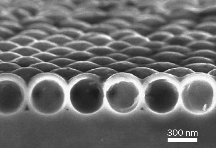
پژوهشگران در امریکا گزارش کرده‌اند که راه جدیدی برای افزایش جذب نوردر لایه‌های نازک ِ یاخته‌های خورشیدی پیدا کرده‌اند. این روش‌ جدید بر مُدهای "دالان نجوا" متکی‌ست که نور را درون پوسته‌های نازک سیلیسیوم به دام می‌اندازند. حاصل کار می‌تواند ابزارهای نورولتایی‌ با بازدهی بیشتر باشد.

نانوبلورهای سیلیسیوم برای ساخت ابزار نورولتایی بسیار مناسبند زیرا به‌خوبی الکتریسیته را هدایت می‌کنند و می‌توانند بدون این‌که آسیب ببینند نور شدید خورشید را تحمل کنند. اما مشکل این است که سیلیسیوم نور را خوب جذب نمی‌کند.. برای افزایش میزان جذب نور باید سیلیسیوم را لایه‌لایه کرد که هم زمان‌ می‌برد و هم پرهزینه است.

اینک یی کویی و همکارانش در دانشگاه استنفورد نشان داده‌اند که نانوپوسته‌های سیلیسیومی راه ساده‌تر و سریع‌تر برای ساخت یاخته‌های خورشیدی‌‌ست. کاواک درون چنین ساختاری نور را در مد "دالان نجوا" حبس می کند. در چنین مدی نور در بسامدهای تشدیدی دقیقی در نتیجه ی بازتاب درونی کامل در لبه ی کاواک دور می گردد. کویی توضیح می دهد که "در عمل نور در این پوسته های توخالی به دام می افتد و مدام دور می گردد به جای آن که عبور کند و این برای کاربردهای نوری بسیار مطلوب است زیرا هرچه نور بیشتر در ماده بماند جذب آن هم بهتر می شود."

گوی‌های سیلیکا
برای ساخت این نانوپوسته‌ها پژوهشگران نخست گوی‌های سیلیکا در اندازه‌های ۵۰ نانومتر ساختند و روی سطحش لایه‌ئی سیلیسیوم نشاندند  سپس با استفاده از هیدروفلوئوریک‌اسید بخش شیشه‌ای‌ی درونی‌ را حل کردند. اسید لایه‌ی سیلیسیوم را نمی‌خورد و به‌این ترتیب پوسته‌ ای سیلیسیومی ساخته می‌شود که به نور حساس است.

این نانوپوسته‌ها را می‌توان طی‌ی چند دقیقه ساخت. در مقایسه برای نشاندن لایه‌ی تخت نانوبلور سیلیسیوم به ضخامت یک میکرون که همان اندازه نور را جذب کند چند ساعت وقت لازم است. طیف جذب نانوپوسته‌ها نیز از طیف جذب لایه‌ی تخت سیلیسیوم گسترده‌تر است. و ماجرا تازه همین جا ختم نمی‌شود:  طبق گفته ی کویی و همکارانش در مقایسه با لایه ی تخت سیلیسیوم به مقدار بسیار کمتری --حدود 5% آن-- ماده برای ساخت نانوپوسته لازم است. واضح است که چنین خصوصیتی هزینه های ساخت را پایین می آورد. " اگر به افق پیش رو بنگریم، این که به میزان بسیار کمتری ماده برای ساخت نانوپوسته نیازاست ممکن است به هنگام تولید انواع دیگر سلول های لایه-نازکی به کار آید، مخصوصا آن ها که از مواد نادر و گرانتر مثل تلوریم و ایندیم استفاده می کنند،"

کاربردهای جدید
این نانوپوسته‌ها حساسیت چندانی هم نسبت به زاویه‌ی فرودی نور ندارند و لایه‌های این نانوپوسته‌ها را می‌توان خم کرد و پیچاند بی آن‌که آسیب ببینند. کویی می افزاید که "همه‌ی این‌ها ممکن است منجر به مجموعه ای از کاربردها در وضعیت‌ها‌ئی شود که نورگیری‌ بهینه از خورشید همیشه ممکن نیست. مثلاً می توانید بادبان‌های نورولتایی را در دریاهای قطبی و یا لباس‌های نورولتایی را برای کوه‌نوردی تصور کنید."

پژوهشگران محاسبات نظری‌ دقیقی را برای این نانوپوسته‌ها کامل کرده اند و اینک مشغول ساخت یاخته‌های واقعی هستند. کویی این را هم آشکار می کند که " ما در حال کاوش در این ساختارها هستیم تا ببینیم آیا می توان از آن ها در کاربردهای دیگری نیز سود جست، از جمله سوخت های خورشیدی و آشکارسازهای خورشیدی." این پژوهش در نشریه‌ی علم ارتباطات نیچر گزارش شده است.

نگراني دانشمندان از كشف تارعنكبوت عجيب در زباله‌هاي هسته‌اي

محققان آمريكايي در حال بررسي تارهاي عنكبوت سفيد رنگ عجيبي هستند كه در استخر زباله‌هاي هسته‌اي كشف شده‌اند. به گزارش پایگاه زیست شناسی ایران، كارمندان بخش زباله هاي هسته‌يي سايت ساوانا ريور در كاروليناي جنوبي ماه گذشته تارهاي عنكبوت عجيبي درعمق 5 و 9 متري استخر سوخت هاي مصرفي پيدا كردند.

چنين ماده سفيد رنگ رشته مانندي تاكنون در بين زباله‌هاي هسته‌اي ديده نشده بود و كشف آن باعث نگراني دانشمندان در خصوص احتمال وقوع جهش ژنتيكي در عنكبوت‌ها شده است. كارشناسان آزمايشگاه ملي ساوانا ريور نمونه‌هاي كشف شده را جمع‌آوري كرده و در حال بررسي دقيق آنها هستند.

اسيديته و دماي آب در استخر سوخت‌هاي مصرفي در اندازه خاصي قرار دارد و در صورت ورود ميكرو ارگانيسم ها به داخل استخر امكان زنده ماندن آنها وجود دارد. حضور هر موجودي در استخر سوخت‌هاي مصرفي، آن را در معرض پرتوهاي راديواكتيو قرار مي‌دهد و احتمال تغييرات ژنتيكي و مبدل شدن به حيوانات بزرگ‌تر را افزايش مي دهد. اگر تارها واقعا توسط عنكبوت‌ها در اعماق استخر درست شده باشند، احتمال قرار گرفتن آنها در معرض پرتوهاي راديواكتيو و جهش ژني عنكبوت وجود دارد.

تنها برخي ارگانيسم‌ها خاصيت مقاومت طبيعي در برابر تابش و پرتوهاي راديواكتيو دارند كه از آن جمله مي‌توان به باكتري «داينوكوكوس راديودورانس» اشاره كرد. اين باكتري يك ارگانيسم طبيعي ضد تابش است كه با استفاده از روش‌هاي مهندسي ژنتيك براي درمان راديواكتيو استفاده مي شود.

تخريب سلول سرطاني با نانوروبات

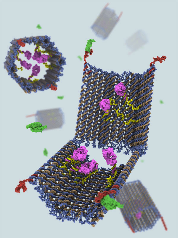
نانوروبات هایی که از اوریگامی (هنر کاغذ و تازدن) DNA ساخته شده اند می توانند به جستجوی سلول های سرطانی پرداخته و آنها را نابود کنند در حالی که سلول های سالم دست نخورده باقی می مانند. این روبات های صدفی شکل که تنها در زمان تشخیص و شناسایی هدف داروهای خود را آزاد می کنند، می توانند در شیوه درمانی سرطان بهبودی قابل توجه ایجاد کنند.

محققان دانشگاه «هاروارد» برای ساخت این نانوروبات ها از اوریگامی DNA استفاده کردند. محققان این روبات را با کمک نرم افزار مدل سازی DNA که می توانست چگونگی اتصال جفت های پایه DNA را درک کند، طراحی کرده و زمانی که شکل مورد نظر خود را به نرم افزار دادند، لیستی از رشته های DNA که با ترکیب آنها شکل مورد نظر به وجود می آمد، ارائه شد.

شکل مورد نظر دانشمندان صدفی بود به این صورت امکان حمل مقادیری دارو در این ساختار به وجود می آمد. دانشمندان برای اطمینان از اینکه دهانه صدف تنها پس از رسیدن به سلول های هدف باز می شوند دو قفل برای آن طراحی کردند که هر یک از آنها رشته ای از DNA هستند که برای شناسایی گونه ای خاص از مولکول ها طراحی شده اند. زمانی که این قفل ها یا «آپتامر»ها به مولکول های هدف می رسند DNA از هم باز شده و دارو آزاد می شود.

عوارض جانبی نانوروبات ها

دانشمندان به منظور آزمودن توانایی های این دارو نانوروبات هایی را مجهز به قفل های شناسایی مولکول های سرطان خون به وجود آورده و دارویی که می تواند با جلوگیری از رشد سلول های این بیماری آنها را نابود کند، درون آن قرار دادند. در نهایت میلیون ها نسخه از این نانوروبات ها در میان سلول های انسانی سالم و سرطانی آزاد شدند.

سه روز بعد نیمی از سلول های سرطانی نابود شده بودند اما هیچ آسیبی به سلول های سالم وارد نیامده بود و دانشمندان دریافتند می توانند با افزودن میزان داروی گنجانده شده در این نانوروبات تمامی سلول های سرطانی را نابود کنند. همچنین با تغییر نوع قفل های دهانه صدف محققان می توانند هر نوع سلول سرطانی را هدف قرار دهند.

داشتن دو قفل به این معنی است که نانوروبات ها از توانایی بالاتری در تشخیص سلول های سرطانی برخوردارند و باید برای آزادسازی دارو دو سیگنال دریافت کنند. محققان امیدوارند نانوروبات ها بتوانند دیگر سلول هایی که در بدن به صورت عادی از رشد سریعی برخوردارند از قبیل سلول های روده و «فولیکول» مو را نیز دست نخورده باقی بگذارند، سلول هایی که معمولا در دوران شیمی درمانی بیشترین آسیب را می بینند.
 
 
                                                            لینک مقاله در وبلاگ

Researchers make single-atom transistor

Researchers in Australia have created a single-atom transistor by planting an individual phosphorus dopant atom within a silicon sample with a spatial accuracy of plus or minus one lattice spacing. The research builds on earlier work by the same group allowing the creation of atomic-scale electrodes. While the transistor may currently help toward the continued miniaturization of classical electronics, the researchers hope that in the future their device will help develop a functional quantum computer.

Moore's Law

The transistor is basically an electronically activated switch and is at the root of all computing. Without it processors would be unable to perform the logical operations required of them. Moore's Law, named after the founder of Intel, Gordon Moore, has predicted that the number of transistors that can be crammed on to a commercial integrated circuit will double approximately every two years. When Moore made his prediction in 1965, he predicted that it would hold true until 1975, when, he suggested correctly, there would be about 65,000 transistors on each chip. In fact, it has proved uncannily accurate and still holds roughly true today, when there are billions. However, continued miniaturization requires the development of new manufacturing techniques, and – for Moore's law to continue – devices will have to hit the single-atom scale around the year 2020.

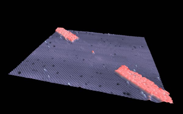
In earlier work, Michele Simmons' research group at the University of New South Wales in Sydney developed a technique allowing it to create atomic wires inside crystals of bulk silicon by selectively removing individual lines of silicon atoms and replacing them with phosphorus. Phosphorus has one more electron in its outer shell than silicon, so replacing a silicon atom with a phosphorus atom within a silicon crystal introduces a free electron to the material and raises the local conductivity. The team used this technique to fashion nanoscale transistor electrodes in the crystal. It then placed a single phosphorus atom in the centre of the transistor. The result was an atomic-scale version of a field-effect transistor (FET).

A quantum transistor

The current passing between the source and drain electrodes of a classical FET increases smoothly with the voltage between the gate and drain electrodes. But the atomic-scale FET produced by the New South Wales group, in collaboration with colleagues at the University of Melbourne, University of Sydney, the Korea Institute for Science and Technology Information and Purdue University in Indiana, US, behaved in a quantum-mechanical manner, becoming conductive only when the potential difference was aligned precisely with one of the energy levels of the phosphorus atom. "You change the bias on the gate and as you change the bias you will access the energy levels of the atom," explains Simmons. "You go from conducting to insulating, to conducting to insulating as you go through the atomistic energy levels of that single-atom device."

Cryogenic laptops and quantum computers

Physicist and electrical engineer David Ferry of Arizona State University in Tempe, US, believes the work is "another interesting example of making a very small structure and placing phosphorus atoms where they want them on a surface". But he questions whether a transistor that can only carry one electron at a time will ever run fast enough to be of much use to the electronics industry. There are also other practical difficulties with the device, such as that it only works with cryogenic refrigeration. As Ferry says, "I don't think you want to carry your laptop around at liquid-helium temperatures."

Simmons accepts that the technology is not currently industrially compatible. "It is really a test of technology," she says. "How far can you push things to deterministically make a single-atom device? Its long-term applicability to conventional industry is completely unknown: it just gives a marker in the sand that there is technology to be able to make it."

The group's main interest in using the transistor was to study the energy levels of the phosphorus atom within the silicon lattice, which the researchers hope to use as qubits in a quantum computer. "This is a transistor that we've designed so that we can look at the energy levels and check that we get agreement with what's been theoretically predicted," says Simmons. "In the computer, the phosphorus atoms will be essentially talking to one another in a lattice. You won't necessarily have source and drain electrodes to each atom like you would in a conventional transistor for that device."

DNA nanorobot delivers drugs

Researchers in the US have developed a new nanorobotic device based on DNA that can deliver "cargo", such as drugs, to individual biological cells. The technology might one day be used to treat various diseases by directly programming the immune response of cells.

The nanorobot, developed by Shawn Douglas and colleagues of the Wyss Institute for Biologically Inspired Engineering at Harvard University, US, is in the form of a hexagonal DNA "hinged" barrel that can be opened and closed. The device measures 35 × 35 × 45 nm and can hold various types of cargo – such as metal nanoparticles – in its interior. It is kept closed by two "locks" that are encoded with aptamers – artificial nucleic-acid receptor molecules that bind to specific target molecules, like some antigens – and can be opened like an oyster shell when it interacts with the right combination of antigen "keys". These keys can be proteins on biological cell surfaces and can be made to include specific disease markers, explains Douglas.

Logical locks

The nanorobot can be programmed to open when exposed to a single type of key by using the same aptamer sequence on both lock sites. Another possibility is to encode different aptamer sequences in the locks to recognize two inputs. Both locks need to be opened at the same time to activate the device and it remains firmly shut if only one of the two locks is opened. The lock mechanism thus functions as a logical AND gate: cell-surface antigens either bind ("0") or do not bind ("1") to aptamer locks.

The barrel was made using "DNA origami" in which complex 3D shapes and objects are constructed by folding strands of DNA. Such a technique has already been used to make nano-sized boxes, which are also capable of carrying cargo, with lids that can be locked and unlocked.

"When the nanorobot opens, its previously sequestered biologically active payload can then interact with nearby cells," explains Douglas. "By designing the lock to open when bound to a particular antigen available on a cell surface, the device can thus be targeted to induce cell-signalling 'instructions' in certain cell populations that express the antigen. At the same time, the cargo is prevented from interacting with other cells [that do not express the antigen] in the same environment."

Instructing cancer cells

The researchers have already used their device to deliver instructions, encoded in antibody fragments, to two different types of cancer cells – those responsible for leukaemia and lymphoma. "The instructions were different for both types of cancer cell and contained different antibody combinations," explains Douglas, "and in each case, the message was to activate the cells' 'suicide switch' – a standard feature that allows ageing or abnormal cells to destroy themselves."

The device is the first DNA-origami-based system that employs antibody fragments to convey molecular instructions, something that allows for a completely controlled and programmable way to replicate an immune response, says team leader, George Church. "We are now finally able to integrate sensing and logical computing functions via complex, yet predictable nanostructures," he states. "These are some of the first hybrids of structural DNA, antibodies, aptamers and metal atomic clusters aimed at useful, very specific targeting of human cancers."

The team now plans to test its device on rodents before considering human clinical trials. "Its applications are possibly not just restricted to smart therapeutics but may also be used in diagnostics and even nonmedical applications," adds Church.