Virtual phonons get real

An acoustic analogue of the dynamical Casimir effect (DCE) has been demonstrated for the first time. Carried out by physicists in France, the experiment involves converting quantum fluctuations into pairs of quantized sound waves – or phonons – in an ultracold atomic gas. The experimental system could boost our understanding of how radiation emerges spontaneously from a vacuum. Indeed, the team is keen on modifying the set-up so it could be used to simulate Hawking radiation, a type of spontaneous vacuum radiation that is created at the edge of black holes.

One of the more peculiar aspects of quantum mechanics is that the vacuum is never truly empty. Instead it contains a small amount of energy and is buzzing with particles that appear out of nothingness, only to vanish again. One famous consequence of this is the Casimir force, where two parallel mirrors positioned close together in a vacuum experience an attractive force. While the force was first proposed in 1948 by the Dutch physicist Hendrik Casimir, it is so small that it was not measured in the lab until 1997.

Separating virtual particles

In 1970 the American physicist Gerald Moore proposed the dynamical Casimir effect, which builds on Casimir's original mirror system and shows how these virtual photons could be converted into real photons. The idea is that the phase of an electromagnetic wave goes to zero at the surface of a mirror. However, if the mirror is accelerated to a significant fraction of the speed of light, the electromagnetic field does not have time to adjust. The result is that the mirror can separate the virtual particles before they annihilate – keeping them in existence long enough to be detected. However, accelerating the mirrors to these speeds in the laboratory has so far proved impossible. To get around this problem, Chris Wilson and colleagues at Chalmers University used a superconducting quantum interference device (SQUID) as an oscillating mirror – and in 2011 they claimed the first demonstration of the DCE in the laboratory.

Now Chris Westbrook and colleagues at the Charles Fabry Laboratory at the University of Paris-Sud say they have created the first acoustic analogue to the DCE – which involves virtual phonons rather than photons. Their experiment was inspired by theoretical work done in 2010 by Iacopo Carusotto of Italy's University of Trento and colleagues. The Italian physicists argued that an acoustic dynamical Casimir effect should be seen in a Bose–Einstein condensate (BEC) when there is a rapid change in the scattering length that governs how its constituent atoms interact. A BEC is formed when identical bosons – particles with integer spin – are cooled until all particles are in the same quantum state. BECs are a good place to look for quantum effects because their extremely low temperature minimizes the effects of thermal noise.

Changing the speed of sound

The team created its BEC by cooling about 100,000 helium atoms to about 200 nK. Instead of changing the scattering length, the team found it could achieve the DCE by changing the speed of sound within the BEC. This was done by squeezing the BEC through rapidly increasing the intensity of the laser that traps the atoms.

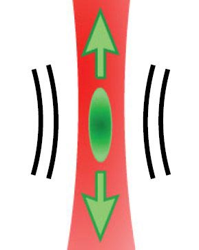
This compression causes virtual phonons to become pairs of real phonons that propagate in opposite directions. These phonons cannot be detected directly. Instead the physicists switch off the laser and then measure the velocity of the atoms as they leave the cloud. This showed that excitations with equal and opposite momenta were moving through the BEC – excitations that were not seen when the BEC was not squeezed.  "Before I started doing this, I had heard of [the dynamic Casimir effect] and it sounded...unfathomably complicated," says Westbrook. "Doing this shows that it is not. It is a concrete illustration of what can happen. And once you can get your mind around it you can start modifying the conditions and thinking about other things [like] Hawking radiation."

Gobbling up sound

In 2009 Jeff Steinhauer and colleagues at the Israel Institute of Technology in Haifa produced an acoustic analogue to a black hole, which gobbles up sound instead of light. Westbrook says the team is particularly interested in combining the two systems to eventually create an acoustic analogue to Hawking radiation, a type of spontaneous vacuum radiation that takes place near the edge of black holes.

One potential flaw of the new experiment is that the DCE is seeded by thermal noise in the BEC – not by quantum vacuum fluctuations. This is because even at a chilly 200 nK, thermal effects are significant and therefore it could be argued that this experiment does not demonstrate the "pure" dynamical Casimir effect. Steinhauer agrees that the goal should be to detect correlated phonons that are seeded by quantum fluctuations. But he says the research is a "good step" toward that goal.

Daniele Faccio at Heriot Watt University in Edinburgh, UK, agrees that the most important next step is for the team to lower the temperature of the BEC. However, Faccio says he feels that the current work is still a demonstration of the physics of the DCE. "It is still a spontaneous emission of radiation, and it is a spontaneous emission that is being generated by a periodic changing boundary condition. So the physics are there," says Faccio. "I think it is a beautiful piece of work. It is extremely useful."

New formula explains the dynamics of fractal growth over time

A team of researchers in Spain says that it has developed an equation that describes how intricate surface patterns, resembling a cauliflower-like motif, evolve and develop over time. The researchers also show that their theory can be applied to everything from actual cauliflower plants to combustion fronts, all of which obey the same scaling laws. The team says that it is the first time that a theoretical explanation has been provided for the growth of surfaces in systems that are extremely dissimilar, be it their physical nature or the scale at which they grow. The researchers based their study, published in New Journal of Physics, on two central tenets: fractals and universality. A fractal is an object or a quantity that is self-similar, or almost so, on all scales. The object need not exhibit exactly the same structure at all scales, but the same "type" of structures must appear on all scales. With a cauliflower, for example, it is impossible to tell if a close-up image of it is the entire head of the cauliflower or just a single floret. Simply put, a fractal is a system where any one part is similar to the whole.

Similar systems

Universality, on the other hand, refers to any physical systems that "look" extremely similar despite their specific details or the scale at which their effects are felt being very different. And fractals are a great example of universality – everything from a single fern leaf that resembles the entire plant, to clouds, snowflakes, blood vessels and cauliflowers has a similar fractal pattern. But despite the properties of fractals, such as their shapes and sizes, having been studied extensively since the 1970s, the physical mechanics of their formation have remained elusive.

Nanocauliflowers

The new work has been carried out by Mario Castro and colleagues from Comillas Pontifical University, Universidad Carlos III de Madrid, Instituto de Ciencia de Materiales-CSIC, Ecole Polytechnique and Katholieke Universiteit Leuven. Initially, the researchers did not start out looking at fractals, instead they were studying a widely used technique to grow thin films known as chemical vapour deposition (CVD), which allows the thickness and composition of layers to be accurately controlled. The team was looking at the evolution of various films grown in the lab and found that one of the films – an amorphous hydrogenated carbon film – had an extremely recognizable if peculiar pattern, namely that of a cauliflower.

Inside joke

The team initially thought that its cauliflower motif was just that – a random pattern that had caught the eye. "It used to be our private joke almost – we used to call them our nanocauliflowers," says Castro, who adds that although the films resemble cauliflowers, they are much smaller, being just several hundreds of nanometres. "But then we realized that our nanocauliflowers also had the same self-similar fractal features as those of the plant," he adds.  Through experiments on its CVD carbon films, the team studied the cauliflower-like fronts, and developed a statistical formula that explains how these fronts grow over time. It turns out that this equation can also be used to successfully predict the growth of an actual cauliflower plant or even a combustion front – or how a flame grows over time – both of which occur at larger and different scales but obey the same scaling laws. "This proves our theory over seven orders of magnitude in length scales," says Castro.

Ingredient's list

The key finding in this work, according to the team, is the identification of the four ingredients needed for the formation of this kind of random growth. The first is a system that grows in time. This is crucial to the second part, which is "non-locality" or competition – a growing system, such as a plant trying to grow taller to receive more sunlight or even part of a flame expanding in time and trying to reach oxygen to combust. The non-locality plays a part here, as what happens in one part of the system remotely affects other distant parts of the same system. The third ingredient is randomness, which, according to the team, nature provides in abundance. The final ingredient is self-similarity – a fractal pattern, where the parts are similar to the whole. "In spite of the widespread success of fractal geometry to describe natural and artificial fractal shapes, purely geometrical descriptions do not provide insight into the laws that govern the emergence of the shapes in time," Castro told physicsworld.com. "We believe that by knowing the general laws that dictate how these patterns form and grow, it will help to identify the biological and physical mechanisms that are at play." The team hopes its work will inspire other researchers to look into the real-world dynamics of fractals, instead of only their morphology.

Invisibility cloaking goes thermodynamic

Researchers in France have shown how to isolate or "cloak" objects from sources of heat – a breakthrough that could help cool down electronic devices and thereby pave the way towards more powerful computers. They also show how the same technique could be used to concentrate heat, which might prove useful in advanced solar technologies.

Invisibility cloaks are based on the mathematics of transformation optics – bending light such that it propagates round a space, rather than through it – and were proposed by John Pendry of Imperial College in London and Ulf Leonhardt of the University of St Andrews in 2006. Now, Sebastien Guenneau of the University of Aix-Marseille and colleagues at the French national research council (CNRS) wondered whether a similar thing could be done with heat. While intuitively, it might seem unlikely that the same mathematics could be applied to thermal diffusion, given that heat does not propagate as a wave but simply diffuses; the researchers found that the transformed equation worked.

Adapting optics

To devise the specific transformations for a thermal invisibility cloak, they considered the heat from a hot object flowing from the left to the right in two dimensions, with the intensity of the heat flux through any region in space represented by the distance between "isotherms" – lines of constant temperature in that region. The more closely spaced the isotherms, the higher is the intensity of the flux. The researchers then transformed the geometry of these isotherms so that they went around rather than through a circular region that is to the right of the heat source, meaning that any object placed in this region would now be shielded from the heat flow.

The invisibility cloak that is needed to achieve this transformation would be a 2D ring built up from many concentric layers of varying diffusivity – a property that reveals how quickly a material conducts heat relative to its heat capacity per unit volume. In their calculations, the researchers modelled a cloak with an inner radius of 200 µm and an outer radius of 300 µm, and then calculated the change in heat flow around the cloak on the order of milliseconds. Because these are the kinds of distances and times relevant to the operation of microelectronic devices such as transistors, the researchers believe that this kind of cloak could be used to protect such devices from unwanted temperature gradients.

Thermal isolation

At larger scales another possible application, says Guenneau, is shielding objects from thermal-imaging cameras. Warm objects such as humans or vehicles can be seen at night using infrared imagers because their black-body spectra peak in the infrared. Putting such an object inside the kind of invisibility cloak devised by the French group would mean isolating it thermally from the outside and therefore concealing any temperature difference between it and the local environment, making the technology of particular interest to the military.

Designing a heat concentrator, on the other hand, which follows from an earlier proposal by Pendry to build concentrators for light, involves calculating the transformation that can divert the isotherms into a central region, rather than away from it. Such concentration of heat into a small space could prove useful in solar energy, says Guenneau, because it could improve the heat exchangers used for instance in concentrated solar-energy systems.

Cloak fabrication

Guenneau and co-workers are now collaborating with scientists at the University of Lille, France, to build these actual devices, in what they hope will be within a matter of months. As Guenneau explains, it ought to be far easier to build a thermal rather than an electromagnetic cloak because the broad range of diffusivities needed to bend the path of heat such that it almost completely bypasses an object can be found in nature. On the other hand, electromagnetic cloaking relies on the fabrication of completely artificial materials made up of extremely small and complex structures.

The 20 concentric layers that make up both the cloak and concentrator will have to be made from a few different materials with various diffusivities, such as metal (which, being a conductor, is highly diffusive) and polymer (which is weakly diffusive). Testing the devices will then involve placing them next to a 500-µm-long resistor and imaging the resulting distribution of heat flux using a thermal camera. If these tests all go to plan, says Guenneau, the step after that would be to make 3D devices.

Other researchers agree that the cloak and concentrator designed by the French group could in principle be built. Tomas Tyc of Masaryk University in the Czech Republic says that their works benefit from a "rigorous adaptation of the method of transformation optics to the diffusion equation". Pendry, meanwhile, says that possible applications might include "Heat sinks that grab excess heat produced by a device, channel it away from sensitive areas and safely dump it into a heat bath."

The research is to be published in an Optical Society of America journal.

نانوپوسته ها برای افزایش بازدهی یاخته‌های خورشیدی

پژوهشگران در امریکا گزارش کرده‌اند که راه جدیدی برای افزایش جذب نوردر لایه‌های نازک ِ یاخته‌های خورشیدی پیدا کرده‌اند. این روش‌ جدید بر مُدهای "دالان نجوا" متکی‌ست که نور را درون پوسته‌های نازک سیلیسیوم به دام می‌اندازند. حاصل کار می‌تواند ابزارهای نورولتایی‌ با بازدهی بیشتر باشد.

نانوبلورهای سیلیسیوم برای ساخت ابزار نورولتایی بسیار مناسبند زیرا به‌خوبی الکتریسیته را هدایت می‌کنند و می‌توانند بدون این‌که آسیب ببینند نور شدید خورشید را تحمل کنند. اما مشکل این است که سیلیسیوم نور را خوب جذب نمی‌کند.. برای افزایش میزان جذب نور باید سیلیسیوم را لایه‌لایه کرد که هم زمان‌ می‌برد و هم پرهزینه است.

اینک یی کویی و همکارانش در دانشگاه استنفورد نشان داده‌اند که نانوپوسته‌های سیلیسیومی راه ساده‌تر و سریع‌تر برای ساخت یاخته‌های خورشیدی‌‌ست. کاواک درون چنین ساختاری نور را در مد "دالان نجوا" حبس می کند. در چنین مدی نور در بسامدهای تشدیدی دقیقی در نتیجه ی بازتاب درونی کامل در لبه ی کاواک دور می گردد. کویی توضیح می دهد که "در عمل نور در این پوسته های توخالی به دام می افتد و مدام دور می گردد به جای آن که عبور کند و این برای کاربردهای نوری بسیار مطلوب است زیرا هرچه نور بیشتر در ماده بماند جذب آن هم بهتر می شود."

گوی‌های سیلیکا
برای ساخت این نانوپوسته‌ها پژوهشگران نخست گوی‌های سیلیکا در اندازه‌های ۵۰ نانومتر ساختند و روی سطحش لایه‌ئی سیلیسیوم نشاندند  سپس با استفاده از هیدروفلوئوریک‌اسید بخش شیشه‌ای‌ی درونی‌ را حل کردند. اسید لایه‌ی سیلیسیوم را نمی‌خورد و به‌این ترتیب پوسته‌ ای سیلیسیومی ساخته می‌شود که به نور حساس است.

این نانوپوسته‌ها را می‌توان طی‌ی چند دقیقه ساخت. در مقایسه برای نشاندن لایه‌ی تخت نانوبلور سیلیسیوم به ضخامت یک میکرون که همان اندازه نور را جذب کند چند ساعت وقت لازم است. طیف جذب نانوپوسته‌ها نیز از طیف جذب لایه‌ی تخت سیلیسیوم گسترده‌تر است. و ماجرا تازه همین جا ختم نمی‌شود:  طبق گفته ی کویی و همکارانش در مقایسه با لایه ی تخت سیلیسیوم به مقدار بسیار کمتری --حدود 5% آن-- ماده برای ساخت نانوپوسته لازم است. واضح است که چنین خصوصیتی هزینه های ساخت را پایین می آورد. " اگر به افق پیش رو بنگریم، این که به میزان بسیار کمتری ماده برای ساخت نانوپوسته نیازاست ممکن است به هنگام تولید انواع دیگر سلول های لایه-نازکی به کار آید، مخصوصا آن ها که از مواد نادر و گرانتر مثل تلوریم و ایندیم استفاده می کنند،"

کاربردهای جدید
این نانوپوسته‌ها حساسیت چندانی هم نسبت به زاویه‌ی فرودی نور ندارند و لایه‌های این نانوپوسته‌ها را می‌توان خم کرد و پیچاند بی آن‌که آسیب ببینند. کویی می افزاید که "همه‌ی این‌ها ممکن است منجر به مجموعه ای از کاربردها در وضعیت‌ها‌ئی شود که نورگیری‌ بهینه از خورشید همیشه ممکن نیست. مثلاً می توانید بادبان‌های نورولتایی را در دریاهای قطبی و یا لباس‌های نورولتایی را برای کوه‌نوردی تصور کنید."

پژوهشگران محاسبات نظری‌ دقیقی را برای این نانوپوسته‌ها کامل کرده اند و اینک مشغول ساخت یاخته‌های واقعی هستند. کویی این را هم آشکار می کند که " ما در حال کاوش در این ساختارها هستیم تا ببینیم آیا می توان از آن ها در کاربردهای دیگری نیز سود جست، از جمله سوخت های خورشیدی و آشکارسازهای خورشیدی." این پژوهش در نشریه‌ی علم ارتباطات نیچر گزارش شده است.

انواع آشكارساز آناليز براي ميكروسكوپ الكتروني

آشکارسازهاي آناليز که در ميکروسکوپ‌هاي الکتروني استفاده مي‌گردد، انواع مختلفي دارند. در اين مقاله سعي شده است به صورت اجمالي مزاياي نسبي آشکارسازهاي موجود، مورد بررسي قرار گيرد. اين آشکارسازها عبارتند از: EDAX) EDS،(WDX) WDS ،AES (اوژه) و EELS که به شرح زير بررسي مي‌شوند:

- آناليز سريع و راحت (در هر بار آزمايش) (بدليل بزرگي زواية فضايي آشكاساز و جمع‌آوري همة پرتوهاي X با انرژي مختلف دريك زمان)
- آناليز كيفي (خطوط نزديكتر از ev 200-100 قابل آشكارسازي نيستند) (علاوه بر درهم رفتن دو پيك مجاور نسبت ارتفاع پيك‌ها به زمينه خيلي خوب نيست)
- ارتفاع پيك به زمينه نامناسب (براي استفاده در اندازه‌گيري‌هاي كمي) (به دليل پارازيت‌هاي الكتروني موجود در آشكارساز)
- محدوديت عنصري (Na به بالا يا B به بالا) (به دليل جذب فوتون‌هاي كم انرژي توسط پنجره‌ها)
- مشكلات سرد بود دائم آشكارساز (شارژ دائمي نيتروژن مايع)
- در برخي نمونه‌ها (تقريباً مشخصند) پيك‌هاي نويزگونه (نويز مجموع دو فوتون و نويز گريزKeV 74/1 E-) وجود دارد كه تشخيص اين پيك‌هاي نويزي نيازمند تجربة تحليلگر يا قدرت نرم‌افزار تحليل كننده دارد.
- امكان تهية همزمان نقشه‌هاي چندگانه (در WDS يگانه) از چند عنصر در يك ناحيه (بر خلاف WDS)
- تنها آشكارسازي كه بر روي TEM و STEM قابل نصب است (البته به شرطي كه اين مسالة در هنگام طراحي TEM و لنزها در نظر گرفته شده باشد) (به دليل تعداد بسيار كم فوتون‌هاي X و راندمان بسيار بالاتر آشكارسازي نسبت به WDS) (از مزاياي نصب EDS بر روي TEM به جاي SEM بالا رفتن تفكيك‌پذيري نقشة به دست آمده از فوتون‌هاي X (تا 10 نانومتر هم مي‌تواند باشد در حالي كه در SEM بهتر از 1 نمي‌تواند باشد)

- سرعت نسبتاً كند ( به دليل كوچكي زاوية فضايي آشكارسازي و جمع‌آوري فقط يك طول موج در آن واحد و در نتيجه لزوم جمع‌آوري ديتا در تمام زواياي ممكن)
- آناليز كمي با دقت بالا:
• تيز بودن پيك‌ها (تشخيص عناصر با انرژي فوتون X نزديك به هم و نادر بودن همپوشاني پيك‌هاي مجاور)
• زياد بودن نسبت ارتفاع پيك‌ به زمينه (اندازه‌گيري كمي غلظت عناصر با دقت خوب 10 برابر EDS)
- لزوم مهندسي دقيق در طراحي دستگاه به دلايل:
• حساسيت بالاي قدرت سيگنال فوتو‌نهاي X به جابجايي و خروج ميكرومتري نمونه از دايرة رولاند (در نتيجه براي به دست آوردن نقشة شيميايي نواحي بزرگتر از 5 × 5 بايد نمونه جابه‌جا شود نه باريكة الكتروني)
• لزوم دقت تنظيم زواياي و 2 با دقت بهتر از 1 دقيقه براي تشخيص خطوط نزديك به هم
- عدم محدوديت آشكارسازي عنصري (به شرط امكان استفاده از چند كريستال، با ثابت شبكه مختلف، در هنگام آناليز طيفي)‌ (به دليل محدوديت‌هاي عملي در طراحي مكانيكي دستگاه در چرخش‌هاي زياد)
- سرعت معقول آشكارسازي هنگامي كه نوع عنصر را از قبل بدانيم (براي آناليز كمي و نقشه عنصر مربوطه) (چرا كه زاوية در مقدار خاصي ثابت نگه داشته مي‌شود و از طرفي سرعت آشكارسازي تعداد فوتون‌ها توسط آشكارسازگازي WDS زياد است)
- تفكيك‌پذيري غلظتي بهتر از EDS است (%05/0 در برابر % 1/0)

توجه
1- دستگاه مخصوصي در بازار وجود دارد (EPMA) كه براي آناليز حرفه‌اي نمونه‌هاي متعدد طراحي شده است.
2- آناليزگرهاي پرتو X هر دو (EDS و WDS) اين مشكل را دارند كه براي نمونه‌هاي ناهموار خيلي مناسب نيستند چرا كه بلندي‌ها بعضاً جلوي رسيدن فوتون‌هاي X جاهاي گود را مي‌گيرند.
3-در برخي ازموارد هر دو آشکارساز بطور همزمان بر روي دستگاه نصب ميشود .

- نياز به خلأ بالا (torr 8-10 )، آسيب‌ديدگي نمونه‌هاي حساس (برخي تركيبات آلي و بيولوژيك)
- مي‌تواند به عنوان آشكارسازي روي SEM نصب شود و نقشة شيميايي سطح را با دقت عرضي 100 نامتر (15 نانو متر در FEAES) و دقت عمقي 3 نانومتر به دست دهد.
- زمان آناليز كامل طيفي هر پيكسل حدود 5 دقيقه
- قابليت تشخيص همة عناصر و تركيبات شيميايي آنها (به جز هليم و هيدروژن) با دقت غلظتي ~ % 30 تا % 10 (و به روايت Evans %1 تا % 1/0 )

- در TEM نصب مي‌شود چرا كه الكترون‌هاي عبوري مورد بررسي قرار مي‌گيرند و ضخامت نمونه بايد كمتر از 100 نانومتر باشد.
- براي عناصر سبك مناسبتر است.
- سرعت نسبتاً كمي دارد ولي استفاده از آشكارسازهاي آرايه‌اي (چيزي شبيه CCDها) اين مساله را كمرنگ مي‌كند.
- براي آناليز كمي نياز به زمان بالاي جمع‌آوري اطلاعات دارد (براي كافي شدن آمار الكتروني)
- در صورت كافي بودن آمار آشكارسازي الکترون ها ضخامت نمونه و تركيب شيميايي عناصر (علاوه بر نوع عنصر و غلظت آن) هم قابل تعيين است.

لینک منبع مقاله

کشف دمای نهایی انجماد آب

به نظر شما آب در چه دمایی یخ می‌زند؟ دانشمندان که می‌گویند الزاماً صفر درجه نیست. در دماهای پایین‌تر از این هم آب می‌تواند حالت مایع خود را حفظ کند که در این‌صورت اصطلاحاً حالت "فروتافته" (Supercooled) به‌خود می‌گیرد.
 
 
به‌گفته دانشمندان، این نوع از آب، نه تنها در صفر درجه یخ نمی‌بندد که می‌تواند تا دمای منفی ۴۸ درجه سلسیوس هم به همان حالت مایع بماند. بر اساس این پژوهش، اگر بخواهید آب را به یخ بدل کنید، به نوعی "بذر یخ" نیازمندید. یعنی بلور ریزی که به‌عنوان هسته و مرجع تجمع دیگر بلورها به شمار می‌آید، اما تولید یخ از آب کاملاً خالصی که در آن هیچگونه آلودگی بیرونی یا ذره‌ای که نقش هسته رسوبی یخ‌ را ایفا کند دیده نمی‌شود، به‌واسطه رفتارهای ترمودینامیکی نامعمول مولکول H2O، کار ساده‌ای نیست.
 
والریا مولینلو (Valeria Molinelo)، شیمیدانی از دانشگاه یوتا و سرنویسنده مقاله مرتبطی است که امروز در نشریه علمی nature انتشار یافته. وی معتقد است تغییر ساختاری آب از حالت مایع به نوعی "یخ واسط"، توصیفی قابل قبول از "چیزی که نقطه انجماد آب را تعیین می‌کند"، به دست می‌دهد. او می‌گوید: "این یخ واسط، چیزی مابین ساختار کامل یک یخ و ساختار سیال یک مایع است. ما مشغول حل معمای دیرینه اتفاقاتی هستیم که در آب فروتافته در جریان است."
 
آب مایع، شبکه‌ای به‌هم‌پیوسته از مولکول‌های آب است که خود از دو اتم هیدروژن و یک اتم اکسیژن ایجاد شده‌اند و با پیوند سستی موسوم به "پیوند هیدروژنی" که چیزی شبیه به کشش ناچیز ناشی از الکتریسیته ساکن است، در این شبکه به هم ارتباط پیدا کرده‌اند. به‌گفته مولینلو، یخ آب، بسته به دما و فشاری که در آن واقع شده است، شانزده شکل بلوری متفاوت دارد که هرکدام‌شان شامل آرایش متمایزی از پیوندهای هیدروژنی می‌شوند. او می‌افزاید: "چیزی که آب را جالب توجه کرده این است که نوع رفتار آب مایع از دیگر انواع مایعات متفاوت است. مثلاً یخ روی آب شناور می‌ماند، حال‌آن که اکثر جامدات، در محیط مملو از حالت مایع‌شان ته‌نشین می‌شوند، چراکه چگال‌ترند». اما چگالی آب از دمایش تبعیت می‌کند و حداکثر آن در دمای ۳.۸ درجه سلسیوس رخ می‌دهد. به همین‌واسطه هم ماهی‌ها در برکه‌ پوشیده از یخ همچنان زنده می‌مانند، چراکه به دیگر کلام، آب برکه گرم‌تر و البته پرچگال‌تر است، اما به‌گفته مولینلو، "جذاب‌ترین ویژگی آب این است که می‌توان تا دماهای زیر صفر درجه هم سردش کرد، حال‌آنکه حالت مایعش از بین نمی‌رود."
 
تا به‌حال، آب فروتافته را تا دمای منفی ۴۱ درجه نگه‌داشته‌اند، اما دانشمندان از مدت‌ها پیش معتقدند که حداقل دمای ممکن این حالت، از این هم کمتر است. البته آن‌ها نمی‌توانند این عدد را مشخص کنند، چراکه در این دما آب با چنان سرعتی یخ می‌زند که تعیین ویژگی‌های آب باقی‌مانده در اطرافش محال است. مولینلو و همکارش امیلی مور (Emily Moore) از دانشگاه یوتا، با کمک شبیه‌سازی‌های رایانه‌ای، دست به بازسازی رفتار آب فروتافته در مقیاس‌های میکروسکوپی زدند. نرم‌افزارشان، رفتارهای ۳۲۷۶۸ مولکول آب را به‌هنگام سرد شدن تقلید می‌کرد و ظرفیت گرمایی، چگالی و سطح تراکم‌پذیری‌شان را نیز همزمان محاسبه می‌نمود. پس از چندین‌هزار ساعت محاسبه مشخص شد دمایی که در آن آب، بی‌برو برگرد از حالت مایع خود به یخ بدل می‌شود، منفی ۴۸ درجه سلسیوس است.
 
وقتی آب به چنین دمایی نزدیک می‌شود، چگالی‌اش کمتر و لذا ساده‌تر می‌شود آن را فشرده کرد و به‌علاوه ساختارش دچار تغییر می‌شود. در نتیجه هر مولکول آب، پیوند سستی را با چهار مولکول کناری برقرار می‌کند و یک چهاروجهی یا هرم را تشکیل می‌دهد. یخ واسط نیز چیزی مابین ساختار شیمیایی مایع و ساختار کامل یک یخ است.
 
این پژوهش، چیزی بیشتر از یک کنجکاوی علمی است. هواشناسانی که با مقوله زمین‌گرمایی دست به گریبان‌اند، بایستی از دمای دقیقی که در آن آب یخ می‌زند و حالت بلوری به خود می‌گیرد، اطلاع داشته باشند. آب، تا دماهای منفی ۴۰ درجه هم در ابرها دیده می‌شود. مولینلو می‌گوید: "برای تخمین مقادیر مایع یا جامد موجود در ابرها، به این دما نیازمندید. این دما، نقش مهمی را در پیش‌بینی‌های مربوط به اقلیم جهانی به خود اختصاص می‌دهد."
 

عدسی های قابل کنترل ساخته شده از حباب‌های گرافین

حباب کوچکی از گرافین می تواند، یک عدسی اپتیکی با فاصله کانونی قابل‌تنظیم بسازد. این ادعای فیزیکدانان در انگلستان است که نشان داده اند، انحنای چنین حباب‌هایی می تواند با اعمال ولتاژ خارجی کنترل شود. ابزارهای ساخته‌شده بر مبنای این کشف می توانند در سامانه‌هایی با کانون تطبیقی استفاده گردد تا نحوه کار چشم انسان را شبیه‌سازی کنند. گرافین لایه‌ای از کربن است که تنها یک اتم ضخامت دارد و ویژگی‌های بی مانند مکانیکی و الکترونیکی را داراست. بسیار کشسان است و می تواند تا 20% کشیده شود؛ یعنی با تورم آن میتواند حباب‌هایی با شکل های متفاوت را تولید کند. این امر در کنار این‌که گرافین ضمن اینکه برای نور شفاف است برای اکثر مایعات و گازها ناتراوا است، باعث می‌شود ماده‌ای ایده‌آل برای ساخت عدسی‌های کانونی تطبیقی باشد.

چنین عدسی‌هایی در دوربین های گوشی‌های تلفن همراه، وب‌کم‌ها و عینک‌های خود فوکوس به کار می‌روند و معمولا از بلورهای مایع یا سیالات شفاف ساخته می‌شود. اگرچه جنین ابزارهایی به‌خوبی کار می‌کنند، ساخت آن‌ها نسبتا دشوار و گران است. در اصل، اپتیک تطبیقی بر پایه گرافین، می‌تواند با استفاده از روش‌های بسیار ساده تری نسبت به ابزارهای موجود، ساخته شود. همچنین، اگر فرایندهای تولید ابزارهای گرافینی در مقیاس صنعتی میسر شود، می‌توان آن‌ها را ارزان‌تر تولید کرد.

حباب‌های بسیار کوچک

اکنون آندری گیم(Andre Geim) و کونستانتین نووسلوف(Konstantin Novoselov) – که جایزه نوبل فیزیک 2010(1389 ه.ش) را به خاطر کشف گرافین با یکدیگر تقسیم کردند- ابزارهای بسیار کوچکی ساخته‌اند که نشان می‌دهد چگونه گرافین می تواند در سامانه‌های اپتیک تطبیقی استفاده گردد. آن‌ها به همراه همکارانشان در دانشگاه منچستر، در ابتدا پوسته‌ی بزرگی از گرافین را روی زیرلایه های اکسید سیلیکون تخت قرار دادند. سپس هوایی از زیر دمیده می شود که نمیتواند از گردافین فرار کند و حبابی از ماده به طور طبیعی شکل می گیرد. حباب ها به شدت پایدار است و اندازه‌ قطرشان از چند ده نانومتر تا ده ها میکرومتر است.

برای نشان‌دادن این که حباب‌ها می‌توانند به عنوان عدسی کانونی تطبیقی کار کنند، این تیم ابزارهایی ساخت که حاوی الکترودهای تیتانیوم/طلا متصل به حباب‌ها در آرایشی شبیه ترانزیستور بودند. به این طریق، پژوهشگران قادر بودند تا ولتاژ ورودی را به چینش وارد کنند. در حالی که ولتاژ ورودی از 35- تا 35+ ولت تغییر میکند، آن ها عکس‌های ساختار را از طریق میکروسکوپ نوری تهیه کردند. همان‌طور که انتظار می‌رود، همین‌طور که ولتاژ تغییر می‌کرد، آن‌ها حباب‌هایی دیدند که از حالت به‌شدت خمیده به حالت تخت‌تر بروند.  در واقع پژوهشگران می‌گویند، عدسی‌ها در حالی کار می‌کردند که حباب‌های گرافین با مایعی با ضریب بازتاب بالا پر شده یا حباب‌ها با لایه تختی از این مایع پوشانده شده بودند. در مرحله بعد چه؟ نووسلوف می گوید: «ما نشان داده‌ایم که کنترل خمش این حباب‌ها کار ساده‌ای است. ما اکنون به دنبال آزمایش‌های دیگری هستیم که تغییر شکل‌های پیچیده تری در گرافین ایجاد کند.»

لینک منبع مقاله

طراحی شبکه‌های کریستالی

طراحی و ایجاد ساختارهای پیچیده و بسیار ریزی که در طبیعت بدون اعمال نیروی خارجی و تنها بر اثر برهم‌کنش‌های داخلی بین مولکول‌ها ساختار خود را منظم می‌کنند، فرایندی بسیار دقیق و پیچیده است.  اگرچه امروزه با پیشرفت علوم می‌توان ذرات را طوری شکل داد که انواع متفاوتی از برهم‌کنش‌ها را با یکدیگر داشته‌باشند، اما وقتی این ذرات در تماس با هم قرار می‌گیرند، پیش‌بینی نوع ساختاری که شکل خواهد گرفت، بسیار دشوار و تقریباً غیر‌ممکن است.اخیراً دو مقاله در مجله Physical review letters چاپ شده که برای طراحی چنین ساختارهایی، روش‌های نظری خوبی ارائه داده‌اند.

ازنظر نظری مطالعه اندرکنش‌های موجود در یک ساختار خاص، برای ایجاد ساختاری شبیه به آن روش مفیدی است و در اغلب موارد پس از انجام این مطالعه محققان از شبیه‌سازی‌های کامپیوتری برای طراحی آن ساختار استفاده می‌کنند. اما اریک ادلوند(Erik Edlund) و همکارانش[1] روش جدیدی را برای طراحی چنین ساختارهایی به کار گرفته‌اند. آن‌ها به جای توصیف برهم‌کنش ذرات در فضای مکان، در فضای اندازه‌حرکت کار کرده و پتانسیل بین ذرات را بدست آوردند. با این روش آن‎‌ها توانستند شکل هندسی حالت پایه انرژی را پیدا کرده و به عنوان تأییدی بر روش خود پتانسیلی را که برای ایجاد یک شبکه مثلثی پیوسته لازم بود بدست آوردند.

در مقاله دوم که توسط همین گروه ارائه شده‌است، به این سؤال پاسخ داده‎‌شده، که وجود نوع خاصی از برهم‌کنش بین ذرات منجر به تشکیل چه نوع ساختارهایی می‌شود؟ برای پاسخ به این سؤال ادلوند و همکارانش مدلی را ارائه دادند که کمترین انرژی ساختاری که برهم‌کنش بین ذرات آن همسانگرد است، را پیش‌بینی می‌کند. آن‌ها نشان دادند که چنین پتانسیلی به یک الفبای محدود برای ساختارهای ممکن منجر می‌شود.

Electron bunches keep their shape

Researchers in Australia have developed a new source of cold electrons that could be useful for imaging tiny structures at atomic-length scales. The source, which makes use of ultracold atoms, can deliver intense and coherent electron pulses with specific shapes – including the Batman motif shown above. According to the team, such pulses could be used in the diffraction imaging of biological molecules, viruses and nanostructures.

Robert Scholten and colleagues at the University of Melbourne begin with a cloud of about one billion rubidium atoms that are laser-cooled to a few millionths of a degree above absolute zero. The team then fires two laser pulses at the atoms. The first pulse puts the atoms in an excited electronic state. The second pulse provides just enough energy to liberate those electrons and create a pulse of cold electrons with a temperature of about 10 K. Electron pulses with complex shapes can be created by passing the first pulse through a spatial light modulator before it strikes the atoms. The pulses are then accelerated to 1 keV using an electric field and then allowed to drift about 21 cm before being detected. Unlike pulses from a conventional, hot-electron source that blur rapidly from the random motion of the electrons, these pulses retain their shapes when detected.

High spatial coherence

Because the electron pulses retain their shape, they have a high degree of spatial coherence perpendicular to their direction of travel. This makes them ideal for diffractive imaging – which the researchers hope to carry out in the coming months. According to Scholten, the transverse coherence length is about 10 nm at the source, which is already good enough to do diffraction imaging of large biomolecules as well as small viruses.

"High spatial coherence means that [the electrons] propagate in a very parallel beam, so when they hit a target, we know where they came from," explains Scholten. "If we then detect them after diffracting from the target, we know where they came from and where they were detected," he adds. This information is used to infer the diffractive effect of the target, which is related to its structure. Such imaging systems would complement existing atomic-force microscopy (AFM) and electron-microscopy techniques.

Being able to shape the pulses should also help researchers get round the phenomenon of "Coulomb explosion", which is a fundamental barrier to creating bright electron pulses. Because electrons have electrical charge, the particles repel each other, thereby causing the pulse to expand as it travels – reducing its intensity. However, if the pulse is created with a specific shape – a uniform-density ellipsoid – Scholten says that it can be refocused using standard electron optics to cancel out the effects of the Coulomb explosion.

"Leapfrog arrangement"

Scholten is quick to point out that the original idea for how to create shaped pulses of cold electrons came from Edgar Vredenbregt, Jom Luiten and colleagues at the Technical University of Eindhoven in the Netherlands. As well as setting out the theory, the Dutch researchers have also worked on electron sources. "We work closely with them and, indeed, they are now adopting the techniques we [have developed], and we are sending them engineering drawings of our system," says Scholten. "It's a leapfrog arrangement – we built on what they did using their experiences and suggestions to progress, and now we are returning the favour."

Thomas Killian of Rice University in Texas tells that "This new work should be viewed as a potential source of electrons that would be used in something like a scanning electron microscope." He describes the work as "a great leap forward" in the development of low source temperatures and long transverse-coherence lengths for the electrons. "I am hopeful that this will accelerate the development of practical tools based on this technology," he adds.

تولید میدان الکتریکی به وسیله ایجاد کشش در لایه‌های درونی ماده

خم کردن برخی از مواد سبب ایجاد میدان الکتریکی می‌شود، پدیده‌ای که به آن اثر فلکسوالکتریک(Flexoelectric) می‌گویند. اخیراً محققان کره‌ای برای دستیابی به این اثر، به جای خم کردن ماده، خمش را در داخل آن رشد داده‌اند و با تغییر درجه خم‌شدگی قدرت میدان الکتریکی را تغییر دادند. این اثر می‌تواند بسیار قوی باشد به طوری که شاید روزی بتوان از آن در نانوحسگرها و یا فعال‌کننده‌های نانومتری استفاده کرد.

اثر فلکسوالکتریک را شاید بتوان از روی اثر پیزوالکتریک(Piezoelectric) شناخت. در اثر پیزوالکتریک وقتی بعضی از مواد فشرده یا کشیده می‌شود، میدان الکتریکی داخلی در آن ایجاد می‌شود. این اثر بسیار مفید، در بسیاری از ابزارها، از میکروسکوپ‌های تونلی (STM) گرفته تا یک فندک، به چشم می‌خورد. اما در کنار این کاربردهای بسیار مفید یک اشکال مهم هم دارد، و آن این است که این اثر تنها می‌تواند در 20 الی 32 ساختار کریستالی با طبقه بندی تقارنی خاص، وجود داشته‌باشد. این در حالی است که چنین محدودیتی برای اثر فلکسوالکتریک وجود ندارد و مواد با هر تقارنی قابلیت بروز چنین پدیده‌ای را دارند. با خم کردن یک کریستال لایه‌های اتمی درون آن کشیده‌می‌شوند و واضح است که بیرونی‌ترین لایه بیشترین کشش را خواهد داشت. این اختلاف کشش در لایه‌های مختلف می‌تواند آنقدر سبب انتقال یون‌ها در کریستال شود که نهایتاً یک میدان الکتریکی در آن ایجاد کند. با این وجود اثر فلکسوالکتریک تا به حال در موادی مانند کریستال‌های مایع، گرافین و حتی مو دیده‌شده‌ بود، و در اجسام جامد خیلی قابل توجه نبوده است.

روشی که محققان کره‌ای، یعنی تائه ون نو (Tae Won Noh) و همکارانش به جای خم کردن یک ماده انعطاف‌پذیر به کار برده‌اند، این است که آن‌ها اختلاف کشش در سطوح مختلف را مستقیماً در داخل کریستال ایجاد کردند. برای ایجاد چنین ساختاری فیلم‌های نازکی از اکسید منگنز هولمیوم(HoMnO3) روی لایه‌ای از یاقوت کبود که فاصله بین انم‌های آن سه و نیم درصد بیشتر از HoMnO3 است، رشد داده‌شد. علت انتخاب HoMnO3 این بود که، این ماده یک فروالکتریک است. فروالکتریک ماده‌ای است که می‌تواند میدان الکتریکی را در خود نگه دارد، درست مثل فرومغناطیس که قابلیت حفظ میدان مغناطیسی را در خود دارد. در فرآیند رشد HoMnO3 روی یاقوت لایه‌ها طوری روی یکدیگر قرار گرفتند که اتم‌های هر لایه کمی از جای اصلی خود جابجا شده‌باشد. در واقع این عمل با استفاده از متراکم کردن اتم‌ها در لایه‌ها متوالی به وسیله بخار انجام شد که باعث می‌شد فاصله اتم‌ها در هر لایه نسبت به لایه زیرین کمتر شود. اما پایداری چنین ساختاری به شدت به اکسیژن موجود در محیط کشت بستگی دارد. کمبود اکسیژن سبب می‌شود تا در طی شکل‌گیری فیلم، فضاهای خالی بسیاری درون آن ایجاد شود و این مسئله قابلیت این ماده را برای متراکم کردن انم‌ها در ضخامت زیاد کاهش می‌دهد. واضح است که در چنین شرایطی فاصله بین اتم‌ها در بیرونی‌ترین لایه خیلی بیشتر از زمانی خواهد بود که اکسیژن بالایی در محیط وجود داشته‌باشد. پراکندگی اشعه ایکس از فیلم‌های با تراکم اکسیژن بالا نشان داد که اختلاف کشش در لایه‌های مختلف، یک تا ده میلیون بار بزرگتر از مقداری است که با خم کردن مواد ایجاد می‌شود. همانطور که ون نو اعتقاد دارد:" با دستیابی به چنین گرادیان کشش عظیمی، در اثر پدیده فلکسوالکتریک یک میدان الکتریکی بسیار یزرگ در ماده ایجاد می‌شود."

به طور معمول، میدان الکتریکی داخل یک ماده فروالکتریک در همه‌جا یکنواخت نیست و در هر ناحیه جهت و راستای خاصی دارد. این گروه از محققان کره‌ای نشان دادند که اثر فلکسوالکتریک در دماهای زیاد و در نمونه‌های با تراکم اکسیژن بالا آنقدر زیاد است که سبب ایجاد یک میدان الکتریکی یکنواخت در سرتاسر ماده می‌شود. اما برای نمونه‌های با اکسیژن پایین که گرادیان کشش کوجکتری دارند چنین پدیده‌ای اتفاق نمی‌افتد. بنابراین با تنظیم میزان اکسیژن در زمان شکل‌گیری این ساختار، می‌توان میدان الکتریکی داخل آن را کنترل کرد و با استفاده از این میدان الکتریکی قادر به تغییر مشخصات فیزیکی این ماده خواهیم بود. ون نو اعتقاد دارد که فیلم‌های با گرادیان کشش بالا از سال‌ها قبل وجود داشته‌اند، اما هیچ‌کس تا به حال به اثر فلکسوالکتریک که داخل آن‌ها وجود داشت توجهی نکرده‌بود.

به اعتقاد گاستئو کاتالان(Gustau Catalan) نتیجه اصلی این آزمایش این است که شرایط جوی در طول رشد فیلم‌ها بر روی پدیده فلکسوالکتریک تأثیر می‌گذارد و با تغییر این شرایط می‌توان خصوصیات فیزیکی یک ماده را عوض کرد.علاوه براین به گفته ون نو همانطور که انتظار می‌رود اثر پزوالکتریک در موتورها و حافظه‌های نانو در آینده کاربردهای مهمی داشته باشد، اثر فلکسوالکتریک نیز ممکن است چنین نقش مهمی را در ساخت این ابزارها ایفا کند.

اختلاف دما در نیم‌ رساناها سبب ایجاد میدان مغناطیسی می‌شود

شبیه سازی‌های کامپیوتری نشان می‌دهد که وجود نواحی سرد و گرم در نیم‌رسانا سبب ایجاد جریان الکتریکی داخلی و درنهایت میدان مغناطیسی می‌شود. اگر این پدیده به طور تجربی در آزمایشگاه تأیید شود، می‌توان از آن در بهبود عملکرد ابزار الکترونیکی که در حین استفاده گرم می‌شوند، سود جست. درواقع کارشناسان هنوز با دید تردید به این اثر می‌نگرند و بحث در مورد اهمیت عملی آن را تا دستیابی به نتایج تجربی به تعویق انداخته‌اند.

به طور کلی اختلاف دما می‌تواند اثرات مهمی روی شارش جریان در نیم‌رسانا داشته باشد، زیرا الکترون‌ها و حفره‌ها تمایل دارند از ناحیه گرم‌تر به ناحیه سردتر شارش پیدا کنند. علاوه براین چنین اثرات گرمایی می‌تواند با میدان‌های مغناطیسی و الکتریکی برهمکنش داشته باشد، که به این پدیده ترموالکترومغناطیس (Thermoelectromagnetic) می‌گویند.

به عنوان مثال، در اثر نرنست (Nernst) وقتی نیم‌رسانا در معرض یک اختلاف دمایی و یک میدان مغناطیسی عمود بر آن قرار می‌گیرد، میدان الکتریکی کوچکی در جهت سوم‌ (یعنی جهتی عمود بر میدان مغناطیسی و اختلاف دمایی)‌ به وجود می‌آید.

جانکیاو (Junqia Wu) و همکارانش در دانشگاه برکلی، متوجه شدند که در پدیده ترموالکترومغناطیس، میدان مغناطیسی هرگز به عنوان خروجی ایجاد نمی‌شود بلکه همیشه به عنوان یک میدان ورودی و یا میدانی که روی سیستم اعمال می‌شود، وجود دارد و نمی‌دانستند که آیا اگر نیم‌رسانا در معرض یک میدان الکتریکی و یک اختلاف دمایی قرار بگیرد، میدان مغناطیسی در آن ایجاد می‌شود یا خیر. بنابراین دو نمونه نیم‌رسانا (در حد ابعاد میکرون) شامل یک نیم‌رسانای نوع  [n] و یک نیم‌رسانای نوع  [p] را شبیه‌سازی کردند، به طوری که نیم‌رسانای نوع n را روی نیم‌رسانای نوع p قرار دادند. با این کار نزدیک سطح جداکننده این دو، یک ناحیه بدون بار و خنثی به وجود می‌آید. زیرا الکترون‌ها و حفره‌های نزدیک این سطح به طرف یکدیگر حرکت کرده و یکدیگر را خنثی می‌کنند. بقیه بارهایی که در هردو نیم‌رسانا وجود دارند و از سطح جداکننده دور هستند، یک میدان الکتریکی به طرف پایین ایجاد می‌کنند. در ادامه در این شبیه‌سازی، یک اختلاف دما در دو سر این مجموعه ایجاد کردند، به این صورت که دمای سمت چپ مجموعه 10 میلی کلوین کمتر و سمت راست 10 میلی کلوین بیشتر از دمای اتاق باشد. با اعمال این شرایط در هردو نیم‌رسانا جریان‌های گردابی ایجاد شد. در نیم‌رسانای نوع n که در بالا قرار داشت الکترون‌ها در لبه بالایی به سمت راست و در بالای سطح جداکننده به سمت چپ حرکت کردند. همین اتفاق در نیم‌رسانای نوع p رخ داد با این تفاوت که جریان به وسیله حفره‌ها ایجاد شد و جهت جریان نیز مخالف جهت جریان در نیم‌رسانای نوع n بود. چنین جریانی باعث ایجاد یک میدان مغناطیسی می‌شود که جهت آن به طرف خارج صفحه است. درواقع این جریان‌ها حاصل شبیه‌سازی‌های بسیار پیچیده کامپیوتری هستند و توضیح چگونگی به وجود آمدن آن‌ها توسط پارامترهای فیزیکی دشوار است. به طور خلاصه و نه خیلی دقیق می‌توان اینطور توضیح داد که نیمی از حلقه جریان در ناحیه بدون بار و خنثی قرار دارد، یعنی ناحیه‌ای به فاصله حدوداً 100 نانومتر از سطح جداکننده، که تقریباً خالی از بارهای الکتریکی است. این کمبود بار سبب می‌شود که اثر اختلاف دمایی در این منطقه زیاد باشد و باعث حرکت بیشتر بارهای متحرک از سمت راست به چپ شود. در نواحی دورتر از این ناحیه یعنی نزدیک لبه بالایی و پایینی مجموعه، رسانایی الکتریکی بسیار بالایی وجود دارد و این باعث می‌شود که بارها حرکت چپ به راست داشته‌باشند.

علاوه براین همانطور که جانکیاو می‌گوید: میدان الکتریکی عمودی به طور مؤثر روی مرکز ابر الکترون و یا حفره اثر می‌کند در حالی که گرادیان دما روی مرکز جرم اثر می‌کند و این نیروهای عمود برهم که نقطه اثرهای متفاوتی دارند سبب ایجاد گشتاور روی بارها می‌شوند. که این استدلال تا حدودی چرخش را توجیه می‌کند. اثری که به صورت تئوری در سال 2005 توسط عده‌ای از فیزیکدانان توضیح داده شد.[3] از طرف دیگر او اعتقاد دارد اگر این مجموعه در یک مدار قرار داده شود جریان‌های گردابی می‌تواند سبب اتلاف انرژی شود و این اثر در ابزارهای الکترونیکی که در حین استفاده گرم می‌شوند ممکن است سبب کاهش بازدهی شود. اما راه حلی نیز برای این مشکل پیشنهاد می‌کند و آن این است که در طراحی ابزار الکترونیکی جریان‌های گردابی را با تنظیم جهت گرادیان دما و میدان الکتریکی به حداقل برسانیم. در واقع درک بهتری از ارتباط بین دما، جریان و میدان‌های الکترومغناطیسی، به مهندسین در بهبود طراحی ابزار الکترونیکی در آینده کمک خواهد کرد.

لینک منبع

Cooling with heat

A quantum system can be cooled with a blast of hot incoherent light. That's the surprising conclusion of theoretical physicists in Germany who have shown that the rate of cooling can sometimes be increased by putting a system in contact with a hot entity. The scheme – which has not been tested in the lab – could offer a simple way of cooling quantum devices.

Since the 1980s physicists have been cooling gases of atoms using coherent laser light. This method works by having atoms absorbing and emitting photons such that the atoms gradually loose momentum. This technique only works if the light is coherent – if it isn't coherent the light simply heats up the gas.

But now Jens Eisert and Andrea Mari of the Freie Universitaet Berlin have come up with a way of using incoherent light to cool a quantum system. Their system is a mechanical quantum oscillator that is coupled to two optical modes – however Eisert stresses that it can be applied to a wide range of three mode quantum systems.

Hot and cold modes

The process begins with the mechanical oscillator in a high-energy or hot state. One of the optical modes is cold, which means that energy can potentially flow from the oscillator to the cold mode – cooling the oscillator.

The second optical mode is hot, meaning that it contains a large number of incoherent photons and is subject to thermal fluctuations. According to Eisert and Mari's calculations, this hot mode has two effects on the temperature of the mechanical oscillator. One effect is obvious; the hot mode heats the oscillator. The second unexpected effect is that fluctuations in the hot mode increase the rate at which energy is transferred from the oscillator to the cold mode. The key to a practical application of the technique is to ensure that the latter effect is dominant.

Eisert says that the system is similar to a transistor, whereby the application of heat at the hot optical mode results in a proportional increase in the flow of heat from the mechanical oscillator to the cold mode.

According to Eisert several experimental groups are now working on realizing the system in the lab. Possible applications of the effect include cooling quantum devices such as atomic clocks or tiny mechanical resonators using incoherent light from relatively inexpensive LEDs.

Flowing electrons magnetize graphene

Physicists in the UK have discovered another useful property of graphene – the material can be magnetized by simply passing a current of electrons through it. The effect could prove useful in creating spintronic or quantum-information devices that use the spin of the electron.

Graphene is a honeycomb-like 2D sheet of carbon just one atom thick. It acts as a semi-metal and is often touted as a "wonder material" with the potential to make extremely small electronic devices of the future.

This latest work was done by Andre Geim and Konstantin Novoselov at the University of Manchester in the UK, who shared the 2010 Nobel Prize for Physics for creating the first sheets of graphene. The research also involved scientists in the US, Russia, Japan and the Netherlands.

Spin currents

The researchers made their discovery by passing an electrical current along a piece of graphene in the presence of a small magnetic field. They found that spin-up and spin-down currents are produced in opposite directions, perpendicular to the direction of the electrical current. The effect is to magnetize the graphene sheet (see figure). The effect is important because it offers physicists a way of controlling spin using electrical current.

The researchers studied more than 20 devices, with two types of graphene – graphene grown on an oxidized silicon wafer and another system where crystals of hexagonal boron nitride were placed between the graphene and the silicon wafer.

While this is not the first time a form of graphene has been magnetized, it is the first time that net magnetization has been created in graphene using spin currents. The research also suggests that spins can be generated, even if graphene has no magnetic moment.

"The central [result] is that they can create large spin currents, which allow them to separate spatially the up and the down spins," says Markus Mueller, at the Abdus Salam International Centre for Theoretical Physics in Italy. Mueller believes that the experiment offers a way to produce simple and robust spin-current sources, which could have many applications.

Imbalance at the Dirac point

Mueller explains that the effect is related to an unusual property of graphene – a Dirac or "neutrality" point where the valence and conduction bands meet. Particles above the Dirac point and holes below the Dirac point react in opposite ways to a magnetic field. The result is an imbalance explains Mueller. "You have more 'up' spins so that their Fermi surface lies in the particle-like region; and fewer 'down' spins, which at their Fermi level are hole-like. That's all you need to create a strong spin current."

Another peculiarity of graphene is that even a very small concentration of charge carriers will hold the magnetization. This is unlike normal substances in which opposite spins can be induced, but a large number of charge carriers are required to maintain the magnetization. If the concentration of charge carriers is decreased, most materials begin to act as insulators and the magnetization is lost. But as Geim explains, in graphene "the dominant phenomenon [of magnetization] still occurs... it even increases as the concentration of charge carriers is reduced, as it is inversely related and this is a salient feature of graphene".

"Non-local quantum effect"

Another surprising finding is that the spins maintain their orientation for relatively long distances in the graphene – a property that is very desirable for spintronics and quantum-information applications. Antonio Castro Neto of Boston University believes that this "non-local quantum effect" is also related to the Dirac point. Writing in Science, he explains that "close to the Dirac point the charge of the electron behaves incoherently (and hence, classically) but its spin behaves coherently (and thus quantum mechanically)".

Francisco Guinea at the Instituto de Ciencia de Materiales de Madrid says the results are very important for spintronic applications, especially as spin currents can be used to retrieve information stored in magnetic devices. Mueller agrees: "It seems this is a quite interesting way to transfer information to spatially different locations via voltage signals, which are easy to process and detect."

The research is reported in Science 332 328 .

Physicists put a new twist on graphene

Physicists in the US and UK have worked out why different samples of multilayer graphene can have very different electronic properties. The answer, according to the team, lies in the relative rotation between layers and the discovery could lead to a new way of controlling the electronic properties of the material.

Graphene is a freestanding layer of carbon just one atom thick and thanks to its 2D nature has a host of unique electronic properties not seen in thicker carbon films. This includes conduction electrons that appear to travel near to the speed of light and have zero mass – so called Dirac fermions. These and other properties of graphene could make it very useful in making ultrafast electronic devices.

Theory suggests that graphene multilayers several atoms thick should not contain Dirac fermions because electron coupling between layers destroys its 2D nature. However, Dirac fermions have been spotted in some multilayers grown by depositing carbon atoms on surfaces, which has puzzled physicists.

A new angle

Now Eva Andrei and colleagues at Rutger's University, Massachusetts Institute of Technology and the University of Manchester have found that the relative angular orientation between successive layers plays a key role in whether or not a multilayer contains Dirac fermions.

The team creates its multilayer samples by depositing carbon onto a nickel surface. The graphene is then lifted off the surface using chemical and studied using a transmission electron microscope to work out the relative angle between the 2D lattices of each layer.

The presence of Dirac fermions was determined using Landau level spectroscopy, whereby a magnetic field is applied to the material. This causes the electrons in each layer to adopt quantized circular orbits – or Landau levels. The energies of these levels are measured using scanning tunnelling spectroscopy and are distinct for Dirac fermions.

Rotated stacks

The team looked at samples where the orientation of graphene layers was close to the most common stacking scheme (Bernal), whereby successive layers are rotated by 60° to each other. They found that when successive layers were offset by about 22° from Bernal stacking, the electrons behaved just like Dirac fermions found in single layers. However, at much smaller rotation angles of about 4°, the velocity of the electrons had dropped to about 80% of that in a single layer.

Also involved in the research is Andre Geim of the University of Manchester, who shared the 2010 Nobel Prize for Physics for his work on graphene. He speculates that the Dirac fermions are seen because the rotation breaks the spatial symmetry between the layers. This could reduce the coupling between layers, making each layer a 2D system.

A third sample was studied with a rotation angle of about 1.2° and this had no evidence of Dirac fermions.

Changing the angle at will

Andrei now plans to repeat the measurements at different twist angles. "New graphene transfer methods opened up possibilities for designing experiments in which we can change the angle at will and exploit these properties for device applications," she explained. Looking further into the future, Andrei speculates that graphene could be patterned with regions of different twist to create electronic devices.

Sankar Das Sarma of the University of Maryland, who was not involved in the research, described the work as "an important milestone in graphene research" that will encourage physicists to study various properties of twisted graphene. However, he pointed out that "much more experimental work on transport and optical properties would be necessary" before technological applications could be considered.

'Jumping' artificial atom is tracked in real time

Researchers in the US say they are first to watch a macroscopic "artificial atom" jumping between energy levels in real time. The new capability to continuously monitor the energy states of a superconducting quantum bit, or qubit, could help to correct errors in quantum computations, tightening the race between these solid-state systems and quantum computers based on trapped atoms.

An optimal measurement system for quantum computations must meet three tough conditions. For one, it must rarely misidentify states. Second, the measurement can't scramble the qubit's state, which is tricky because quantum states are easy to destroy. And finally, it must be fast – on the timescale of nanoseconds. This is essential for seeing quantum jumps, since many measurements must be made before the qubit changes state.

While these conditions were met 25 years ago for trapped atoms, Rajamani Vijay, Daniel Slichter and Irfan Siddiqi at the University of California, Berkeley are the first to score the hat trick using superconducting qubits – sometimes referred to as artificial atoms because of their discrete energy states.

The team did the experiment inside a cryogenic helium refrigerator cooled to 30 mK. The superconducting qubit is an aluminium circuit, a few hundred microns across but considered macroscopic, and the low temperatures brought out its quantum properties. As a nonlinear electrical oscillator, its energy levels were unevenly spaced. This allows the team to use microwaves at a frequency of 4.753 GHz to drive it only between its ground and first excited states – the qubit's 0 and 1 states.

Revealing and protecting

The researchers connect the qubit to the superconducting microwave cavity, an ordinary harmonic oscillator, through small capacitors. Because of this link, the cavity's preferred photon frequency changes based on the state of the qubit. The cavity could reveal information about the qubit while at the same time protecting it from noise.

To measure the qubit's state, the team generates higher-frequency microwave photons and admits them, no more than about 30 at a time, into the superconducting cavity. There, the photons interact with the qubit and acquire a phase shift depending on the qubit's state – 180° if the qubit is in its excited state, or 0° if it is in the ground state.

Now bearing the qubit's mark, the photons reflect out of the cavity toward the amplifier. Like the qubit, the amplifier is a nonlinear oscillator, this time designed to behave classically. Its superconductivity means low noise since it loses energy as heat.

The amplifier is finely tuned to accept a particular power, or rate of incoming photons, without changing their phase as they reflect back out. This is precisely the power it receives from a microwave source, which generated frequencies matching that of the signal photons.

Minuscule but important

However, in joining this stream of photons on the way to the amplifier, the signal photons exert a minuscule but important influence – adding a tiny bit more power if their phases haven't been shifted, or interfering destructively and slightly reducing the power if they have. The amplifier is so carefully balanced that it senses even this small difference and reacts dramatically. If the power is not what the amplifier expects, it imposes a phase shift of up to 90° in either direction on the photons it reflects. This shift is one way if the qubit is excited and the other way if it is in its ground state.

The amplifier magnifies the original signal from a few photons to hundreds of photons, making it large enough to withstand the noise introduced by common methods for increasing a signal. It also rapidly changes the phase of the photons, speeding up detection. "The combination of low noise and speed was crucial in observing quantum jumps for the first time," says Vijay.

The team extracts the qubit's state every 10 nanoseconds – plenty often enough to monitor the qubit's 320 nanosecond long excited state and notice when it jumped to the ground state. And now that close surveillance on a qubit has been achieved, the method can be set to work correcting errors in quantum computations.

Correcting errors

To do this, a piece of quantum information is stored across multiple qubits. If one of these qubits falls out of its state, the others can still maintain the shared quantum information, as long as the wayward qubit is brought back into line quickly. But up until now, there was no way to continuously monitor a superconducting qubit and catch it making the transition from one state to another.

"Superconducting quantum bits are without doubt one of the hot candidates in the ongoing race towards a full-scale quantum computer," says Jens Koch of Northwestern University in Evanston, Illinois. He calls the new monitoring system "a key step forward".

لینک مقاله

نوبل فیزیک 2010 برای کشف کامل‌ترین ماده روی زمین

جایزه نوبل فیزیک 2010 به طور مشترک به دو استاد دانشگاه منچستر در انگلیس به خاطر مطالعات نوآورانه‌شان در مورد گرافن رسید. گرافن، ماده‌ای جدید با کامل‌ترین ساختار بلوری است که دریچه تازه‌ای را در نانوتکنولوژی گشورده است.
آکادمی سلطنتی علوم سوئد، تصمیم گرفت جایزه نوبل فیزیک امسال را به آندره گیم و کنستانتین نووسلوف، هر دو از دانشگاه منچستر انگلستان برای آزمایش‌هایی که بر روی ماده دوبعدی گرافن داشتند، اهدا نماید.

کامل‌ترین شبکه اتمی
یک ورقه نازک از کربن معمولی،‌ آن‌هم با ضخامت تنها یک اتم، برنده جایزه نوبل فیزیک امسال را تعیین کرد. اندره گیم و کنستانتین نووسلوف نشان دادند که کربن در این شکل مسطح خاص، ویژگی‌های بسیار متفاوتی دارد که ریشه در دنیای فیزیک کوانتومی دارند.

گرافن در حقیقت همان کربن است، اما به عنوان یک ماده، کاملا جدید است و هم لقب نازک‌ترین و هم لقب قوی‌ترین ماده را از آن خود ساخته است. وقتی پای رسانایی جریان الکتریکی در میان باشد، به اندازه مس رسانا است. اما در رسانایی گرما تمام مواد وجود دیگر را پشت سر می‌گذارد و بالاترین عملکرد را به خود اختصاص می‌دهد.

گرافن تقریبا کاملا شفاف است. با این حال هنوز به اندازه‌ای تراکم دارد که حتی هلیوم که دارای کوچک‌ترین مولکول‌های گازی است، نمی‌تواند از آن عبور کند. با این که تقریبا هر آن‌چه روی زمین مربوط به حیات است و ما می‌شناسیم از کربن منشا گرفته، اما کربن با این شکل جدید خود همه را شگفت‌زده کرده است.

گیم و نووسلوف، گرافن را از یک تکه گرافیت معمولی، مثل همان ماده‌ای که در همه مدادهای معمولی یافت می‌شود،‌ به دست آوردند. آن‌ها با یک نوار چسب معمولی سعی کردند لایه‌ای از کربن را با ضخامت تنها یک اتم به دست بیاورند. در آن زمان بسیاری باور داشتند که این کار غیرممکن است، چراکه تصور می‌کردند ماده‌ای کریستالی با این ضخامت کم نمی‌تواند پایدار باشد.

اما امروز فیزیکدانان می‌توانند با استفاده از گرافن، طبقه تازه‌ای از مواد 2بعدی را که دارای ویژگی‌های خاص خود هستند، مطالعه کنند. گرافن مطالعاتی را ممکن کرده که پیچیدگی‌های تازه‌ای را در دنیای پدیده‌های فیزیک کوانتوم پدیدار می‌کنند. همچنین کاربردهای عملی تازه‌ و بسیار متنوعی بعد از کشف گرافن به راه افتاده، مانند ساخت مواد جدید و تولید ابزار الکترونیکی کاملا نو و ابتکاری. پیش‌بینی می‌شود که ترانزیستورهای گرافنی بسیار سریع‌تر از ترانزیستورهای سیلیکونی عمل کنند و این یعنی ظهور رایانه‌هایی با کارامدی بسیار بالاتر.

از آن‌جایی که گرافن واقعا شفاف است و رسانایی خوبی هم دارد، می‌تواند برای ساخت نمایشگرهای لمسی شفاف، صفحه‌های نوری و شاید حتی صفحه‌های خورشیدی به کار آید.

وقتی گرافن با پلاستیک ترکیب شود، می‌تواند آن‌ را به رسانای الکتریکی تبدیل کند و در حالی که مقاومتش در برابر گرما بالاتر می‌رود، از نظر مکانیکی قوی‌تر هم شود. از این مقاومت می‌توان در مواد جدید فوق قوی استفاده کرد که هم ظریف هستند و هم الاستیک؛ هم انعطاف‌پذیرند و هم از سبکی فوق‌العاده‌ای بهره می برند. در آینده، ماهواره‌ها، هواپیماها و خودروها را می‌توان از این مواد ترکیبی جدید ساخت.

pyb24un75h5vdfvq7ojh.jpg

آشنایی با برندگان
برندگان جایزه نوبل فیزیک امسال برای مدت‌های طولانی روی این پروژه مطالعه و کار کرده‌اند. کنستانتین نووسلوف 36 ساله در ابتدا کار خود را با اندره گیم 51 ساله به عنوان دانشجوی دکتری در هلند آغاز کرد. سپس وی به همراه گیم به انگلستان رفت. هر دوی آن‌ها در اصل کار خود را در روسیه آغاز کرده بودند و حالا هر دو در دانشگاه منچستر استاد هستند.

اندره گیم
متولد سال 1958 در سوشی روسیه. دارنده مدرک دکتری از موسسه فیزیک حالت جامد، آکادمی علوم روسیه،‌ چرنوگولوکا، روسیه، سال 1987. مدیر مرکز مزوساینس و نانوتکنولوژی منچستر. استاد فیزیک و پروفسور تحقیقاتی سال 2010 جامعه سلطنتی،‌ دانشگاه منچستر، ‌انگلستان.

Andre Geim

کنستانتین نووسلوف
متولد سال 1974 در نیژنی‌تاجیل، روسیه. دارنده مدرک دکتری از دانشگاه رادبوند نیجمگان در هلند به سال 2004. استادیار و دستیار پژوهشی جامعه سلطنتی، دانشگاه منچستر، ‌انگلستان.

Konstantin Novoselov

Graphene makes 'supercapacitor

Researchers in the US have made the first high-frequency AC "supercapacitors" containing graphene electrodes. The devices, which are much smaller than conventional capacitors, could be used in applications like computer processing units and other tiny integrated circuits.

Capacitors are devices that store electric charge. "Supercapacitors", more accurately known as electric double-layer capacitors (DLCs) or electrochemical capacitors, can store much more charge thanks to the double layer formed at an electrolyte-electrode interface when voltage is applied.

Commercial DLCs are extremely powerful when compared with batteries but they are essentially DC devices – that is, they take several seconds to fully charge and then several seconds to fully discharge again. They operate efficiently at frequencies below about 0.05 Hz and are therefore good for applications like hybrid vehicles, which can take up to 10 seconds to charge (when braking) and 10 seconds to discharge (when accelerating). However, at higher frequencies, they become much less efficient and start to behave like resistors rather than capacitors. This is because the devices usually contain porous electrodes made from a high-surface-area conductive material, such as activated carbon, and the pores increase the resistance of devices.

Now, John R Miller and colleagues of JME Inc. in Shaker Heights and Case Western Reserve University, Cleveland, both in Ohio, have overcome this problem by developing the first DLC that contains vertically oriented high-surface-area graphene electrodes that aren't porous at all. The device pushes the operating frequency of an electric double layer capacitor to well beyond 5000 Hz, which is a factor of 105 better than commercial DLCs. What's more, it is six times smaller than low-voltage aluminium electrolytic capacitors and can be charged and discharged at high efficiency in times much shorter than 1 ms.

The researchers grew the graphene – 2D sheets of carbon just one atom thick – on a metal using a plasma-assisted chemical vapour deposition process.

Such vertically oriented graphene sheets are ideal in terms of structure for high-frequency DLC electrode applications, says the team. They have many edge planes that can provide between 50 and 70 µF/cm2 of capacitance compared with basal planes, which only provide 3 µF/cm2. These charge-storage edge planes are highly exposed and can thus be accessed directly, which means that charge can be stored over precise areas rather than being dispersed over larger regions. And last but not least, the nanosheet "stacked" structure ensures that pores are reduced – so minimizing resistance – and the sheets themselves are highly conducting.

"The bottom line is that these devices could lead to smaller higher-frequency capacitors for applications in low-voltage systems like CPUs and similar integrated circuits," Miller said.

The research might also enable new classes of electronic circuit that use the much higher levels of capacitance that these devices make available, he adds.

The team, which includes scientists from the College of William and Mary in Williamsburg and the Defense Advanced Research Projects Agency, both in Virginia, now plans to improve how the graphene electrode material is grown and optimize the design of the capacitive devices.

لینک سایت اصلی